参数资料
| 型号: | DS2415P+ |
| 厂商: | Maxim Integrated Products |
| 文件页数: | 2/14页 |
| 文件大小: | 0K |
| 描述: | IC TIME CHIP 1-WIRE 6-TSOC |
| 产品培训模块: | Lead (SnPb) Finish for COTS Obsolescence Mitigation Program |
| 标准包装: | 120 |
| 类型: | 二进制计数器 |
| 特点: | 唯一 ID |
| 时间格式: | 二进制 |
| 数据格式: | 二进制 |
| 接口: | 1 线 串行 |
| 电源电压: | 2.5 V ~ 5.5 V |
| 电压 - 电源,电池: | 2.5 V ~ 5.5 V |
| 工作温度: | -40°C ~ 85°C |
| 安装类型: | 表面贴装 |
| 封装/外壳: | 6-LSOJ |
| 供应商设备封装: | 6-TSOC |
| 包装: | 管件 |
DS2415
10 of 14
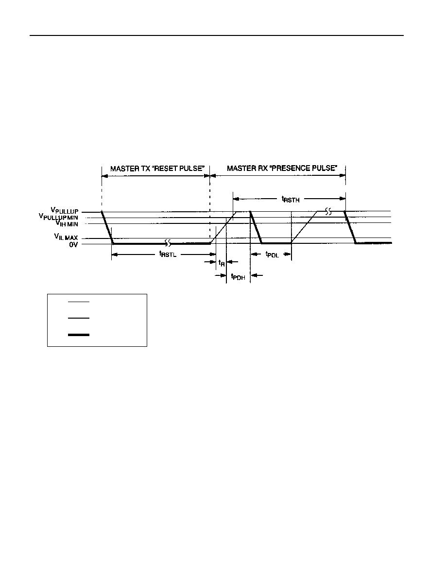
1-WIRE SIGNALING
The DS2415 requires strict protocols to insure data integrity. The protocol consists of four types of
signaling on one line: Reset Sequence with Reset Pulse and Presence Pulse, Write 0, Write 1, and Read
Data. The bus master initiates all these signals, except Presence Pulse. The initialization sequence
required to begin any communication with the DS2415 is shown in Figure 8. A Reset Pulse followed by a
Presence Pulse indicates the DS2415 is ready to send or receive data given the correct ROM command
and control function command. The bus master transmits (TX) a Reset Pulse (tRSTL , minimum 480
ms).
The bus master then releases the line and goes into receive mode (RX). The 1-Wire bus is pulled to a high
state via the pullup resistor. After detecting the rising edge on the data line, the DS2415 waits (tPDH, 15
ms
to 60
ms) and then transmits the Presence Pulse (tPDL , 60ms to 240ms).
INITIALIZATION PROCEDURE “RESET AND PRESENCE PLUSES” Figure 8
480
ms tRSTL < *
480
ms tRSTH < ( INCLUDES RECOVERY TIME)
15
ms tPDH < 60ms
60
ms tPDL < 240ms
* In order not to mask interrupt signaling by other devices on the 1-Wire bus, tRSTL + tR should always
be less than 960
ms.
READ/WRITE TIME SLOTS
The definitions of write and read time slots are illustrated in Figure 9. All time slots are initiated by the
master driving the data line low. The falling edge of the data line synchronizes the DS2415 to the master
by triggering a delay circuit in the DS2415. During write time slots, the delay circuit determines when the
DS2415 will sample the data line. For a read data time slot, if a 0 is to be transmitted, the delay circuit
determines how long the DS2415 will hold the data line low overriding the 1 generated by the master. If
the data bit is a 1, the device will leave the read data time slot unchanged.
RESISTOR
MASTER
DS2415
相关PDF资料 |
PDF描述 |
|---|---|
| AD5116BCPZ5-RL7 | IC DGTL POT 64POS 5K 8LFCSP |
| D38999/24FG16PC | CONN RCPT 16POS JAM NUT W/PINS |
| AD5245BRJZ10-RL7 | IC DGTL POT 256POS SOT-23-8 T/R |
| AD5258BRMZ1-R7 | IC POT DGTL I2C 1K 64P 10MSOP |
| D38999/24FG16PB | CONN RCPT 16POS JAM NUT W/PINS |
相关代理商/技术参数 |
参数描述 |
|---|---|
| DS2415P/T&R | 功能描述:实时时钟 RoHS:否 制造商:Microchip Technology 功能:Clock, Calendar. Alarm RTC 总线接口:I2C 日期格式:DW:DM:M:Y 时间格式:HH:MM:SS RTC 存储容量:64 B 电源电压-最大:5.5 V 电源电压-最小:1.8 V 最大工作温度:+ 85 C 最小工作温度: 安装风格:Through Hole 封装 / 箱体:PDIP-8 封装:Tube |
| DS2415P/T&R-W | 功能描述:实时时钟 RoHS:否 制造商:Microchip Technology 功能:Clock, Calendar. Alarm RTC 总线接口:I2C 日期格式:DW:DM:M:Y 时间格式:HH:MM:SS RTC 存储容量:64 B 电源电压-最大:5.5 V 电源电压-最小:1.8 V 最大工作温度:+ 85 C 最小工作温度: 安装风格:Through Hole 封装 / 箱体:PDIP-8 封装:Tube |
| DS2415P+ | 功能描述:实时时钟 RoHS:否 制造商:Microchip Technology 功能:Clock, Calendar. Alarm RTC 总线接口:I2C 日期格式:DW:DM:M:Y 时间格式:HH:MM:SS RTC 存储容量:64 B 电源电压-最大:5.5 V 电源电压-最小:1.8 V 最大工作温度:+ 85 C 最小工作温度: 安装风格:Through Hole 封装 / 箱体:PDIP-8 封装:Tube |
| DS2415P+T&R | 制造商:Maxim Integrated Products 功能描述:IC TIME CHIP 1-WIRE 6-TSOC |
| DS2415P+T&R | 功能描述:实时时钟 RoHS:否 制造商:Microchip Technology 功能:Clock, Calendar. Alarm RTC 总线接口:I2C 日期格式:DW:DM:M:Y 时间格式:HH:MM:SS RTC 存储容量:64 B 电源电压-最大:5.5 V 电源电压-最小:1.8 V 最大工作温度:+ 85 C 最小工作温度: 安装风格:Through Hole 封装 / 箱体:PDIP-8 封装:Tube |
发布紧急采购,3分钟左右您将得到回复。