- 您现在的位置:买卖IC网 > PDF目录1915 > DS2482X-101+T (Maxim Integrated Products)IC MASTER I2C-1WIRE 1CH 9-WLP PDF资料下载
参数资料
| 型号: | DS2482X-101+T |
| 厂商: | Maxim Integrated Products |
| 文件页数: | 19/24页 |
| 文件大小: | 0K |
| 描述: | IC MASTER I2C-1WIRE 1CH 9-WLP |
| 产品培训模块: | Lead (SnPb) Finish for COTS Obsolescence Mitigation Program |
| 标准包装: | 2,500 |
| 控制器类型: | I²C 总线控制器 |
| 接口: | I²C |
| 电源电压: | 2.9 V ~ 5.5 V |
| 电流 - 电源: | 750µA |
| 工作温度: | -40°C ~ 85°C |
| 安装类型: | 表面贴装 |
| 封装/外壳: | 9-WFBGA,WLBGA |
| 供应商设备封装: | 9-WLP |
| 包装: | 带卷 (TR) |
DS2482-101
Single-Channel 1-Wire Master with Sleep Mode
4
_______________________________________________________________________________________
Note 1:
Operating current with 1-Wire write-byte sequence followed by continuously reading the Status Register at 400kHz in overdrive.
Note 2:
With standard speed, the total capacitive load of the 1-Wire bus should not exceed 1nF. Otherwise, the passive pullup on
threshold VIL1 may not be reached in the available time. With overdrive speed, the capacitive load on the 1-Wire bus must
not exceed 300pF.
Note 3:
Active pullup guaranteed to turn on between VIL1(MAX) and VIH1(MIN).
Note 4:
Active or resistive pullup choice is configurable.
Note 5:
Except for tF1, all 1-Wire timing specifications and tAPUOT are derived from the same timing circuit. Therefore, if one of
these parameters is found to be off the typical value, it is safe to assume that all these parameters deviate from their typi-
cal value in the same direction and by the same degree.
Note 6:
These values apply at full load, i.e., 1nF at standard speed and 0.3nF at overdrive speed. For reduced load, the pulldown
slew rate is slightly faster.
Note 7:
Fall time high-to-low (tF1) is derived from PDSRC, referenced from 0.9 x VCC to 0.1 x VCC.
Note 8:
I2C communication should not take place for the max tOSCWUP or tSWUP time following a power-on reset or a wakeup from
sleep mode.
Note 9:
Guaranteed by design and not production tested.
Note 10: All I2C timing values are referred to VIH(MIN) and VIL(MAX) levels.
Note 11: Applies to SDA, SCL, and AD0.
Note 12: The input/output pins of the DS2482-101 do not obstruct the SDA and SCL lines if VCC is switched off.
Note 13: The DS2482-101 provides a hold time of at least 300ns for the SDA signal (referred to the VIH(MIN) of the SCL signal) to
bridge the undefined region of the falling edge of SCL.
Note 14: The maximum tHD:DAT need only be met if the device does not stretch the low period (tLOW) of the SCL signal.
Note 15: A fast-mode I2C bus device can be used in a standard-mode I2C bus system, but the requirement tSU:DAT
≥ 250ns must
then be met. This is automatically the case if the device does not stretch the low period of the SCL signal. If such a device
does stretch the low period of the SCL signal, it must output the next data bit to the SDA line tR(MAX) + tSU:DAT = 1000 +
250 = 1250ns (according to the standard-mode I2C bus specification) before the SCL line is released.
Note 16: CB—Total capacitance of one bus line in pF. If mixed with high-speed-mode devices, faster fall times according to I2C-
Bus Specification Version 2.1 are allowed.
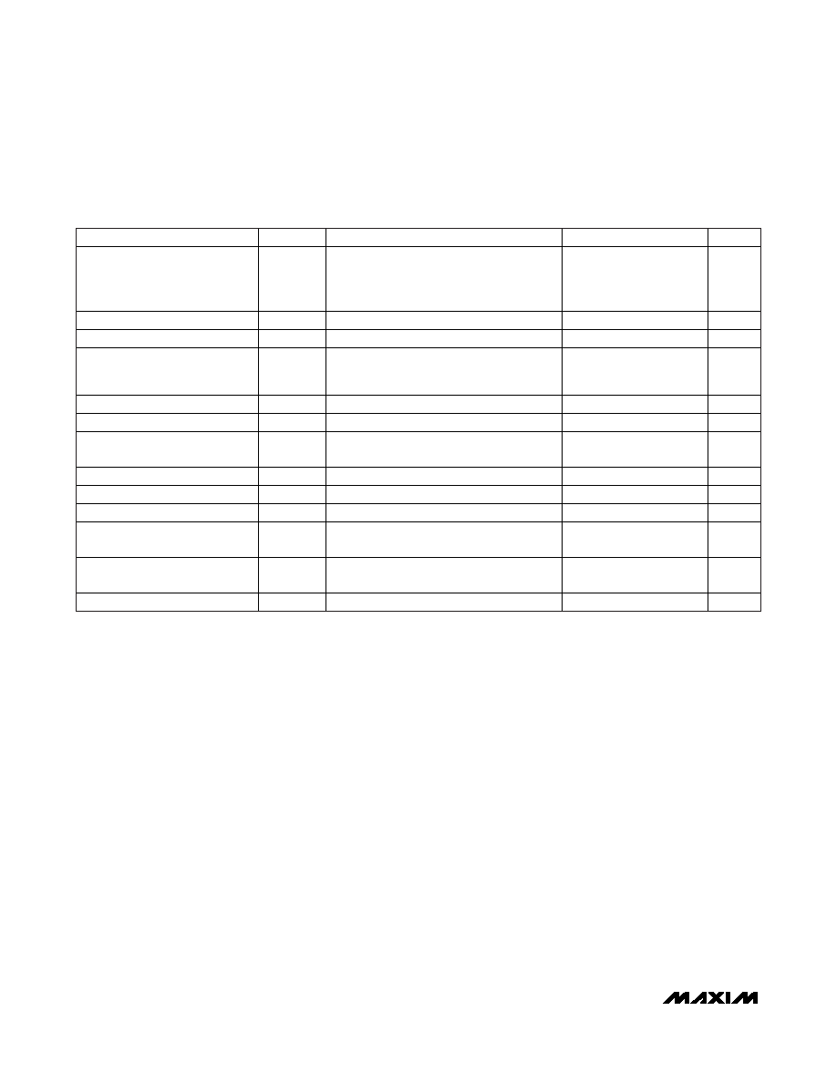
ELECTRICAL CHARACTERISTICS (continued)
(VCC = 2.9V to 5.5V, TA = -40°C to +85°C.)
PARAMETER
SYMBOL
CONDITIONS
MIN
TYP
MAX
UNITS
Input Current Each Input/Output
Pin with an Input Voltage
Between 0.1 x VCC(MAX) and
0.9 x VCC(MAX)
II
(Notes 11, 12)
-10
+10
μA
Input Capacitance
CI
(Note 11)
10
pF
SCL Clock Frequency
fSCL
0
400
kHz
Hold Time (Repeated) START
Condition (After this period, the
first clock pulse is generated.)
tHD:STA
0.6
μs
Low Period of the SCL Clock
tLOW
1.3
μs
High Period of the SCL Clock
tHIGH
0.6
μs
Setup Time for a Repeated
START Condition
tSU:STA
0.6
μs
Data Hold Time
tHD:DAT
(Notes 13, 14)
0.9
μs
Data Setup Time
tSU:DAT
(Note 15)
250
ns
Setup Time for STOP Condition
tSU:STO
0.6
μs
Bus Free Time Between a STOP
and START Condition
tBUF
1.3
μs
Capacitive Load for Each Bus
Line
CB
(Note 16)
400
pF
Oscillator Warmup Time
tOSCWUP
(Note 8)
100
μs
相关PDF资料 |
PDF描述 |
|---|---|
| DS2483Q+T | IC I2C TO 1WIRE BRIDGE 8TDFN |
| DS2490Y | IC BRIDGE CLIP USB TO 1-W 24SOIC |
| DS26303LN-75+A3 | IC LIU E1/T1/J1 3.3V 144-ELQFP |
| DS26324GNA2+ | IC INTERFACE LINE 16CH 256-CSBGA |
| DS26334GN+ | IC INTERFACE LINE 16CH 256-CSBGA |
相关代理商/技术参数 |
参数描述 |
|---|---|
| DS2483 | 制造商:MAXIM 制造商全称:Maxim Integrated Products 功能描述:Single-Channel 1-Wire Master with Adjustable Timing and Sleep Mode |
| DS2483Q+T | 功能描述:I2C 接口集成电路 Single-Channel 1-Wire Master RoHS:否 制造商:NXP Semiconductors 电源电压-最大:5.5 V 电源电压-最小:2.3 V 最大工作频率:400 KHz 最大工作温度:+ 85 C 封装 / 箱体:TSSOP-16 |
| DS2483Q+U | 功能描述:I2C 接口集成电路 SINGLE-CH 1-WIRE MASTER RoHS:否 制造商:NXP Semiconductors 电源电压-最大:5.5 V 电源电压-最小:2.3 V 最大工作频率:400 KHz 最大工作温度:+ 85 C 封装 / 箱体:TSSOP-16 |
| DS2483R+T | 功能描述:I2C 接口集成电路 Single-Channel 1-Wire Master RoHS:否 制造商:NXP Semiconductors 电源电压-最大:5.5 V 电源电压-最小:2.3 V 最大工作频率:400 KHz 最大工作温度:+ 85 C 封装 / 箱体:TSSOP-16 |
| DS2483R+U | 功能描述:接口 - 专用 SINGLE-CH 1-WIRE MASTER RoHS:否 制造商:Texas Instruments 产品类型:1080p60 Image Sensor Receiver 工作电源电压:1.8 V 电源电流:89 mA 最大功率耗散: 最大工作温度:+ 85 C 安装风格:SMD/SMT 封装 / 箱体:BGA-59 |
发布紧急采购,3分钟左右您将得到回复。