- 您现在的位置:买卖IC网 > PDF目录16259 > DS26334DK (Maxim Integrated Products)KIT DESIGN FOR DS26334 PDF资料下载
参数资料
| 型号: | DS26334DK |
| 厂商: | Maxim Integrated Products |
| 文件页数: | 47/121页 |
| 文件大小: | 0K |
| 描述: | KIT DESIGN FOR DS26334 |
| 产品培训模块: | Lead (SnPb) Finish for COTS Obsolescence Mitigation Program |
| 设计资源: | DS26334DK Gerber Files |
| 标准包装: | 1 |
| 主要目的: | 电信,线路接口单元(LIU) |
| 已用 IC / 零件: | DS26334 |
| 已供物品: | 板,线缆,电源 |
第1页第2页第3页第4页第5页第6页第7页第8页第9页第10页第11页第12页第13页第14页第15页第16页第17页第18页第19页第20页第21页第22页第23页第24页第25页第26页第27页第28页第29页第30页第31页第32页第33页第34页第35页第36页第37页第38页第39页第40页第41页第42页第43页第44页第45页第46页当前第47页第48页第49页第50页第51页第52页第53页第54页第55页第56页第57页第58页第59页第60页第61页第62页第63页第64页第65页第66页第67页第68页第69页第70页第71页第72页第73页第74页第75页第76页第77页第78页第79页第80页第81页第82页第83页第84页第85页第86页第87页第88页第89页第90页第91页第92页第93页第94页第95页第96页第97页第98页第99页第100页第101页第102页第103页第104页第105页第106页第107页第108页第109页第110页第111页第112页第113页第114页第115页第116页第117页第118页第119页第120页第121页
DS26334 3.3V, 16-Channel, E1/T1/J1 Short/Long-Haul Line Interface Unit
31 of 121
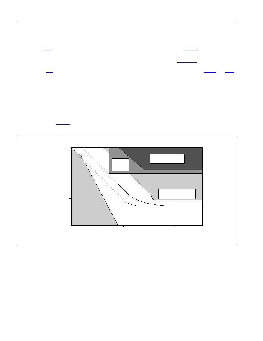
5.6
Jitter Attenuator
The DS26334 contains an on-board jitter attenuator that can be set to a depth of either 32 or 128 bits via the JADS
bit in register GC. It can also be controlled on an individual LIU basis by settings in the IJAFDS register.
The 128-bit mode is used in applications where large excursions of wander are expected. The 32-bit mode is used
in delay sensitive applications. The characteristics of the attenuation are shown in Figure 5-9. The jitter attenuator
can be placed in either the receive path or the transmit path or none by appropriately setting the JAPS and the JAE
bits in register GC. These selections can be changed on an individual LIU basis by settings in the IJAPS and IJAE.
In order for the jitter attenuator to operate properly, a 2.048MHz clock or multiple thereof, or 1.544MHz clock or
multiple thereof, must be applied at MCLK. ITU-T specification G.703 requires an accuracy of ±50ppm for both T1
and E1 applications. AT&T Pub 62411 and ANSI specs require an accuracy of ±32ppm for T1 interfaces. On-board
circuitry adjusts either the recovered clock from the clock/data recovery block or the clock applied at the TCLK pin
to create a smooth jitter-free clock, which is used to clock data out of the jitter attenuator FIFO. It is acceptable to
provide a jittery clock at the TCLK pin if the jitter attenuator is placed on the transmit side. If the incoming jitter
exceeds either 120UIP-P (buffer depth is 128 bits) or 28UIP-P (buffer depth is 32 bits), the DS26334 will divide the
internal nominal 32.768MHz (E1) or 24.704MHz (T1) clock by either 15 or 17 instead of the normal 16 to keep the
buffer from overflowing. When the device divides by either 15 or 17, it also sets the jitter attenuator limit trip
(IJAFLT) bits in the IJAFLT register described.
Figure 5-9. Jitter Attenuation
FREQUENCY (Hz)
0dB
-20dB
-40dB
-60dB
1
10
100
1K
10K
JITTER
ATTENUAT
ION
(d
B)
100K
TR 62411 (Dec. 90)
Prohibited Area
C
ur
ve
B
C
ur
ve
A
ITU G.7XX
Prohibited Area
TBR12
Prohibited
Area
T1
E1
相关PDF资料 |
PDF描述 |
|---|---|
| VE-JWH-EY-S | CONVERTER MOD DC/DC 52V 50W |
| GCC19DREN | CONN EDGECARD 38POS .100 EYELET |
| GBM36DSEH-S243 | CONN EDGECARD 72POS .156 EYELET |
| GCC19DREH | CONN EDGECARD 38POS .100 EYELET |
| GCC20DCST | CONN EDGECARD 40POS DIP .100 SLD |
相关代理商/技术参数 |
参数描述 |
|---|---|
| DS26334G | 功能描述:电信集成电路 3.3V E1/T1/J1 16Ch Short/Long Haul LIU RoHS:否 制造商:STMicroelectronics 类型:Telecom IC - Various 工作电源电压:4.75 V to 5.25 V 电源电流: 工作温度范围:- 40 C to + 85 C 安装风格:SMD/SMT 封装 / 箱体:PQFP-100 封装:Tray |
| DS26334G+ | 功能描述:电信集成电路 3.3V E1/T1/J1 16Ch Short/Long Haul LIU RoHS:否 制造商:STMicroelectronics 类型:Telecom IC - Various 工作电源电压:4.75 V to 5.25 V 电源电流: 工作温度范围:- 40 C to + 85 C 安装风格:SMD/SMT 封装 / 箱体:PQFP-100 封装:Tray |
| DS26334GA2 | 功能描述:电信集成电路 RoHS:否 制造商:STMicroelectronics 类型:Telecom IC - Various 工作电源电压:4.75 V to 5.25 V 电源电流: 工作温度范围:- 40 C to + 85 C 安装风格:SMD/SMT 封装 / 箱体:PQFP-100 封装:Tray |
| DS26334GA2+ | 功能描述:电信集成电路 RoHS:否 制造商:STMicroelectronics 类型:Telecom IC - Various 工作电源电压:4.75 V to 5.25 V 电源电流: 工作温度范围:- 40 C to + 85 C 安装风格:SMD/SMT 封装 / 箱体:PQFP-100 封装:Tray |
| DS26334GA3 | 功能描述:电信集成电路 3.3V E1/T1/J1 16Ch Short/Long Haul LIU RoHS:否 制造商:STMicroelectronics 类型:Telecom IC - Various 工作电源电压:4.75 V to 5.25 V 电源电流: 工作温度范围:- 40 C to + 85 C 安装风格:SMD/SMT 封装 / 箱体:PQFP-100 封装:Tray |
发布紧急采购,3分钟左右您将得到回复。