- 您现在的位置:买卖IC网 > PDF目录1915 > DS26519GN+ (Maxim Integrated Products)IC TXRX T1/E1/J1 16PRT 484-HSBGA PDF资料下载
参数资料
| 型号: | DS26519GN+ |
| 厂商: | Maxim Integrated Products |
| 文件页数: | 212/310页 |
| 文件大小: | 0K |
| 描述: | IC TXRX T1/E1/J1 16PRT 484-HSBGA |
| 产品培训模块: | Lead (SnPb) Finish for COTS Obsolescence Mitigation Program |
| 标准包装: | 30 |
| 类型: | 收发器 |
| 驱动器/接收器数: | 16/16 |
| 规程: | 以太网 |
| 电源电压: | 3.135 V ~ 3.465 V |
| 安装类型: | 表面贴装 |
| 封装/外壳: | 484-BGA 裸露焊盘 |
| 供应商设备封装: | 484-HSBGA(23x23) |
| 包装: | 管件 |
第1页第2页第3页第4页第5页第6页第7页第8页第9页第10页第11页第12页第13页第14页第15页第16页第17页第18页第19页第20页第21页第22页第23页第24页第25页第26页第27页第28页第29页第30页第31页第32页第33页第34页第35页第36页第37页第38页第39页第40页第41页第42页第43页第44页第45页第46页第47页第48页第49页第50页第51页第52页第53页第54页第55页第56页第57页第58页第59页第60页第61页第62页第63页第64页第65页第66页第67页第68页第69页第70页第71页第72页第73页第74页第75页第76页第77页第78页第79页第80页第81页第82页第83页第84页第85页第86页第87页第88页第89页第90页第91页第92页第93页第94页第95页第96页第97页第98页第99页第100页第101页第102页第103页第104页第105页第106页第107页第108页第109页第110页第111页第112页第113页第114页第115页第116页第117页第118页第119页第120页第121页第122页第123页第124页第125页第126页第127页第128页第129页第130页第131页第132页第133页第134页第135页第136页第137页第138页第139页第140页第141页第142页第143页第144页第145页第146页第147页第148页第149页第150页第151页第152页第153页第154页第155页第156页第157页第158页第159页第160页第161页第162页第163页第164页第165页第166页第167页第168页第169页第170页第171页第172页第173页第174页第175页第176页第177页第178页第179页第180页第181页第182页第183页第184页第185页第186页第187页第188页第189页第190页第191页第192页第193页第194页第195页第196页第197页第198页第199页第200页第201页第202页第203页第204页第205页第206页第207页第208页第209页第210页第211页当前第212页第213页第214页第215页第216页第217页第218页第219页第220页第221页第222页第223页第224页第225页第226页第227页第228页第229页第230页第231页第232页第233页第234页第235页第236页第237页第238页第239页第240页第241页第242页第243页第244页第245页第246页第247页第248页第249页第250页第251页第252页第253页第254页第255页第256页第257页第258页第259页第260页第261页第262页第263页第264页第265页第266页第267页第268页第269页第270页第271页第272页第273页第274页第275页第276页第277页第278页第279页第280页第281页第282页第283页第284页第285页第286页第287页第288页第289页第290页第291页第292页第293页第294页第295页第296页第297页第298页第299页第300页第301页第302页第303页第304页第305页第306页第307页第308页第309页第310页
DS26519 16-Port T1/E1/J1 Transceiver
29 of 310
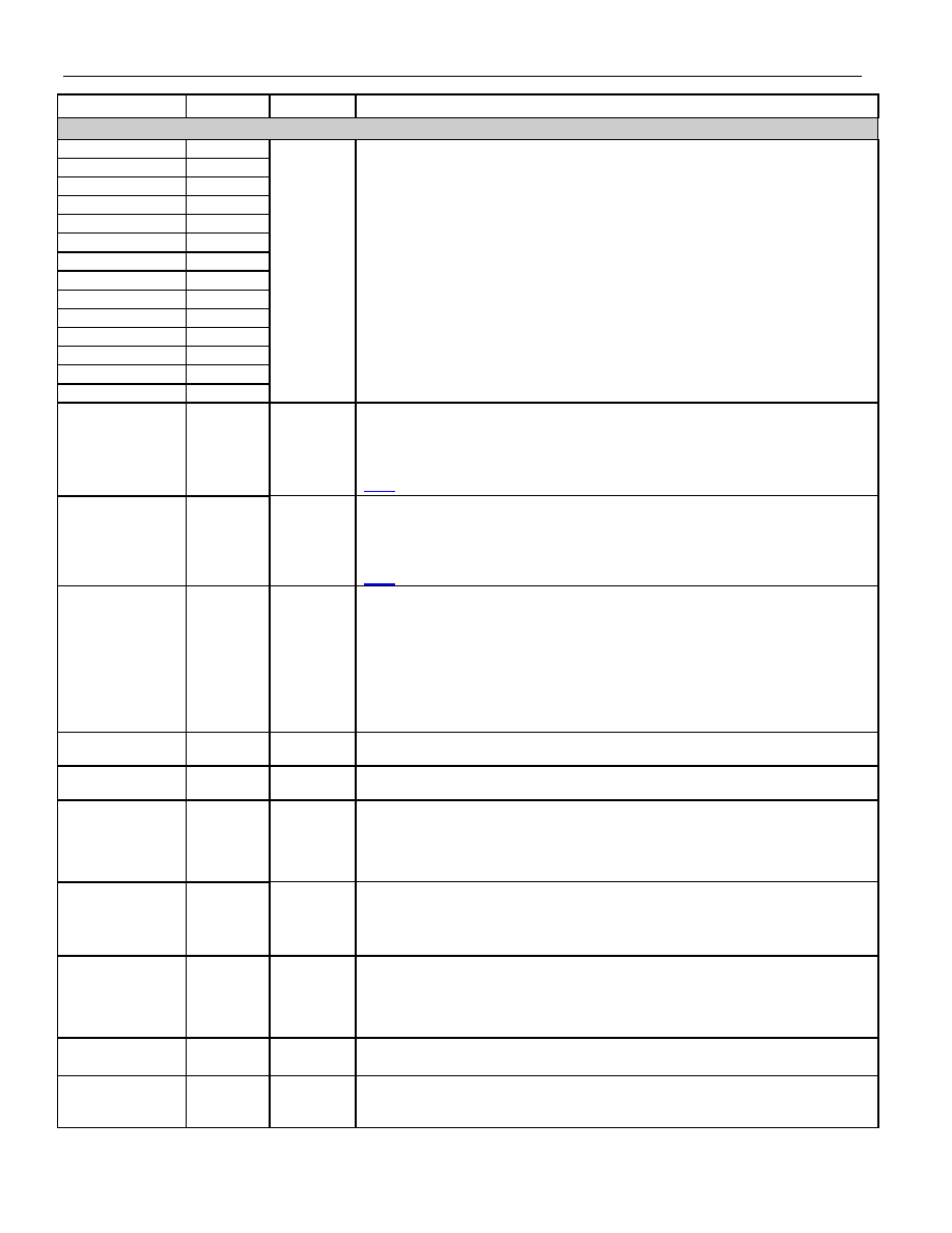
NAME
PIN
TYPE
FUNCTION
MICROPROCESSOR INTERFACE
A13
C16
A12
F12
A11
A20
A10
G11
A9
H9
A8
A21
A7
F13
A6
A22
A5
H10
A4
B19
A3
H11
A2
D15
A1
G13
A0
B20
Input
Address [13:0].
This bus selects a specific register in the DS26519 during
read/write access. A13 is the MSB and A0 is the LSB.
D[7]/
SPI_CPOL
Y9
Input
Data [7]/SPI Interface Clock Polarity
D[7]:
Bit 7 of the 16-bit or 8-bit data bus used to input data during register writes
and data outputs during register reads. Not driven when
CSB = 1.
SPI_CPOL:
This signal selects the clock polarity when SPI_SEL = 1. See Section
9.1.2 for detailed timing and functionality information. Default setting is low.
D[6]/
SPI_CPHA
U8
Input
Data [6]/SPI Interface Clock Phase
D[6]:
Bit 6 of the 16-bit or 8-bit data bus used to input data during register writes
and data outputs during register reads. Not driven when
CSB = 1.
SPI_CPHA:
This signal selects the clock phase when SPI_SEL = 1. See Section
9.1.2 for detailed timing and functionality information. Default setting is low.
D[5]/
SPI_SWAP
AA6
Input
Data [5]/SPI Bit Order Swap
D[5]:
Bit 5 of the 16-bit or 8-bit data bus used to input data during register writes
and data outputs during register reads. Not driven when
CSB = 1.
SPI_SWAP:
This signal is active when SPI_SEL = 1. The address and data bit
order is swapped when SPI_SWAP is high. The R/W and B bit positions are
never changed in the control word.
0 = LSB is transmitted and received first.
1 = MSB is transmitted and received first.
D[4]
T14
Input
Data [4].
Bit 4 of the 8-bit data bus used to input data during register writes and
data outputs during register reads. Not driven when
CSB = 1.
D[3]
AB5
Input
Data [3].
Bit 3 of the 8-bit data bus used to input data during register writes and
data outputs during register reads. Not driven when
CSB = 1.
D[2]/
SPI_SCLK
R14
Input
Data [2]/SPI Serial Interface Clock
D[2]:
Bit 2 of the 8-bit data bus used to input data during register writes and data
outputs during register reads. Not driven when
CSB = 1.
SPI_SCLK:
SPI Serial Clock Input when SPI_SEL = 1.
D[1]/
SPI_MOSI
AA5
Input
Data [1]/SPI Serial Interface Data Master Out-Slave In
D[1]
: Bit 1 of the 8-bit data bus used to input data during register writes, and data
outputs during register reads. Not driven when
CSB = 1.
SPI_MOSI:
SPI Serial Data Input (Master Out-Slave In) when SPI_SEL = 1.
D[0]/
SPI_MISO
P14
Input
Data [0]/SPI Serial Interface Data Master In-Slave Out
D[0]:
Bit 0 of the 8-bit data bus used to input data during register writes and data
outputs during register reads. Not driven when
CSB = 1.
SPI_MISO:
SPI Serial Data Output (Master In-Slave Out) when SPI_SEL = 1.
CSB
W8
I
Chip-Select Bar.
This active-low signal is used to qualify register read/write
accesses. The
RDB/DSB and WRB signals are qualified with CSB.
RDB/
DSB
Y8
I
Read-Data Bar/Data-Strobe Bar.
This active-low signal along with
CSB qualifies
read access to one of the DS26519 registers. The DS26519 drives the data bus
with the contents of the addressed register while
RDB and CSB are low.
相关PDF资料 |
PDF描述 |
|---|---|
| DS26521L+ | IC TXRX T1/E1/J1 64-LQFP |
| DS26522GN+ | IC TXRX T1/E1/J1 DUAL 144CSBGA |
| DS26524GNA5+ | IC TXRX T1/E1/J1 QUAD 256-CSBGA |
| DS26528GNA5+ | IC TXRX T1/E1/J1 OCT 256-CSBGA |
| DS26900LN+ | IC JTAG MUX/SWITCH 144-LQFP |
相关代理商/技术参数 |
参数描述 |
|---|---|
| DS26519GN+ | 功能描述:网络控制器与处理器 IC 16-Port E1/T1/J1 Transceiver RoHS:否 制造商:Micrel 产品:Controller Area Network (CAN) 收发器数量: 数据速率: 电源电流(最大值):595 mA 最大工作温度:+ 85 C 安装风格:SMD/SMT 封装 / 箱体:PBGA-400 封装:Tray |
| DS26519GNA2 | 功能描述:网络控制器与处理器 IC 16-Port E1/T1/J1 Transceiver RoHS:否 制造商:Micrel 产品:Controller Area Network (CAN) 收发器数量: 数据速率: 电源电流(最大值):595 mA 最大工作温度:+ 85 C 安装风格:SMD/SMT 封装 / 箱体:PBGA-400 封装:Tray |
| DS26519GNA2+ | 功能描述:网络控制器与处理器 IC 16-Port E1/T1/J1 Transceiver RoHS:否 制造商:Micrel 产品:Controller Area Network (CAN) 收发器数量: 数据速率: 电源电流(最大值):595 mA 最大工作温度:+ 85 C 安装风格:SMD/SMT 封装 / 箱体:PBGA-400 封装:Tray |
| DS26521 | 制造商:Maxim Integrated Products 功能描述:DS26521 MONOLITHIC T1E1J1 SCT - Rail/Tube |
| DS26521DK | 功能描述:网络开发工具 DS26521 Dev Kit RoHS:否 制造商:Rabbit Semiconductor 产品:Development Kits 类型:Ethernet to Wi-Fi Bridges 工具用于评估:RCM6600W 数据速率:20 Mbps, 40 Mbps 接口类型:802.11 b/g, Ethernet 工作电源电压:3.3 V |
发布紧急采购,3分钟左右您将得到回复。