参数资料
| 型号: | DS32C35-33# |
| 厂商: | Maxim Integrated Products |
| 文件页数: | 3/22页 |
| 文件大小: | 0K |
| 描述: | IC RTC W/TCXO 20-SOIC |
| 产品变化通告: | Product Discontinuation 28/Nov/2011 |
| 标准包装: | 37 |
| 类型: | 时钟/日历 |
| 特点: | 警报器,FRAM,闰年,方波输出,TCXO/晶体 |
| 存储容量: | 8KB |
| 时间格式: | HH:MM:SS(12/24 小时) |
| 数据格式: | YY-MM-DD-dd |
| 接口: | I²C,2 线串口 |
| 电源电压: | 2.7 V ~ 3.63 V |
| 电压 - 电源,电池: | 2.3 V ~ 3.6 V |
| 工作温度: | 0°C ~ 70°C |
| 安装类型: | 表面贴装 |
| 封装/外壳: | 20-SOIC(0.295",7.50mm 宽) |
| 供应商设备封装: | 20-SOIC W |
| 包装: | 管件 |
| 产品目录页面: | 1433 (CN2011-ZH PDF) |
DS32B35/DS32C35
Accurate I2C RTC with Integrated
TCXO/Crystal/FRAM
____________________________________________________________________
11
troller resets, the RTC I2C interface may be placed into
a known state by toggling SCL until SDA is observed to
be at a high level. At that point the microcontroller
should pull SDA low while SCL is high, generating a
START condition.
FRAM
The serial FRAM memory is logically organized as a
2048 x 8 or 8192 x 8 memory array and is accessed
using the I2C interface. Functional operation of the
FRAM is similar to serial EEPROMs with the major dif-
ference being its superior performance on writes. The
memory is read or written at the speed of the I2C inter-
face. It is not necessary to poll the device for a ready
condition during writes.
Due to the different memory densities, the I2C address-
ing technique is different for each version of the device.
See the
I2C Serial Data Bus section for details.
Warning: The FRAM does not inhibit reads or writes
when VCC is below the minimum operating voltage.
FRAM reads are destructive, that is, when a read is
performed, the device internally writes the memory
back to the original value. The FRAM must not be read
or written when VCC is below the minimum operating
voltage; otherwise, the memory cells may not be fully
programmed, and the data may not be retained.
RTC Address Map
Table 3 shows the RTC address map for the timekeep-
ing registers. During a multibyte access, when the
address pointer reaches the end of the register space,
it wraps around to location 00h. On an I2C START or
address pointer incrementing to location 00h, the cur-
rent time is transferred to a second set of registers. The
time information is read from these secondary registers,
while the clock continues to run. This eliminates the
need to reread the registers in case the main registers
update during a read.
Clock and Calendar
The time and calendar information is obtained by read-
ing the appropriate register bytes. Table 3 illustrates the
RTC registers. The time and calendar data are set or ini-
tialized by writing the appropriate register bytes. The con-
tents of the time and calendar registers are in the
binary-coded decimal (BCD) format. The device can be
run in either 12-hour or 24-hour mode. Bit 6 of the hours
register is defined as the 12- or 24-hour mode select bit.
When high, the 12-hour mode is selected. In the 12-hour
mode, bit 5 is the AM/PM bit with logic-high being PM. In
the 24-hour mode, bit 5 is the 20-hour bit (20 to 23 hours).
The century bit (bit 7 of the month register) is toggled
when the years register overflows from 99 to 00.
The day-of-week register increments at midnight.
Values that correspond to the day of week are user-
defined but must be sequential (i.e., if 1 equals
Sunday, then 2 equals Monday, and so on). Illogical
time and date entries result in undefined operation.
When reading or writing the time and date registers, sec-
ondary (user) buffers are used to prevent errors when
the internal registers update. When reading the time and
date registers, the user buffers are synchronized to the
internal registers on any START and when the register
pointer rolls over to zero. The time information is read
from these secondary registers while the clock continues
to run. This eliminates the need to reread the registers in
case the main registers update during a read.
The countdown chain is reset whenever the seconds
register is written. Write transfers occur on the acknowl-
edge from the device. Once the countdown chain is
reset, to avoid rollover issues the remaining time and
date registers must be written within 1 second. The 1Hz
square-wave output, if enabled, transitions high 500ms
after the seconds data transfer, provided that the oscil-
lator is already running.
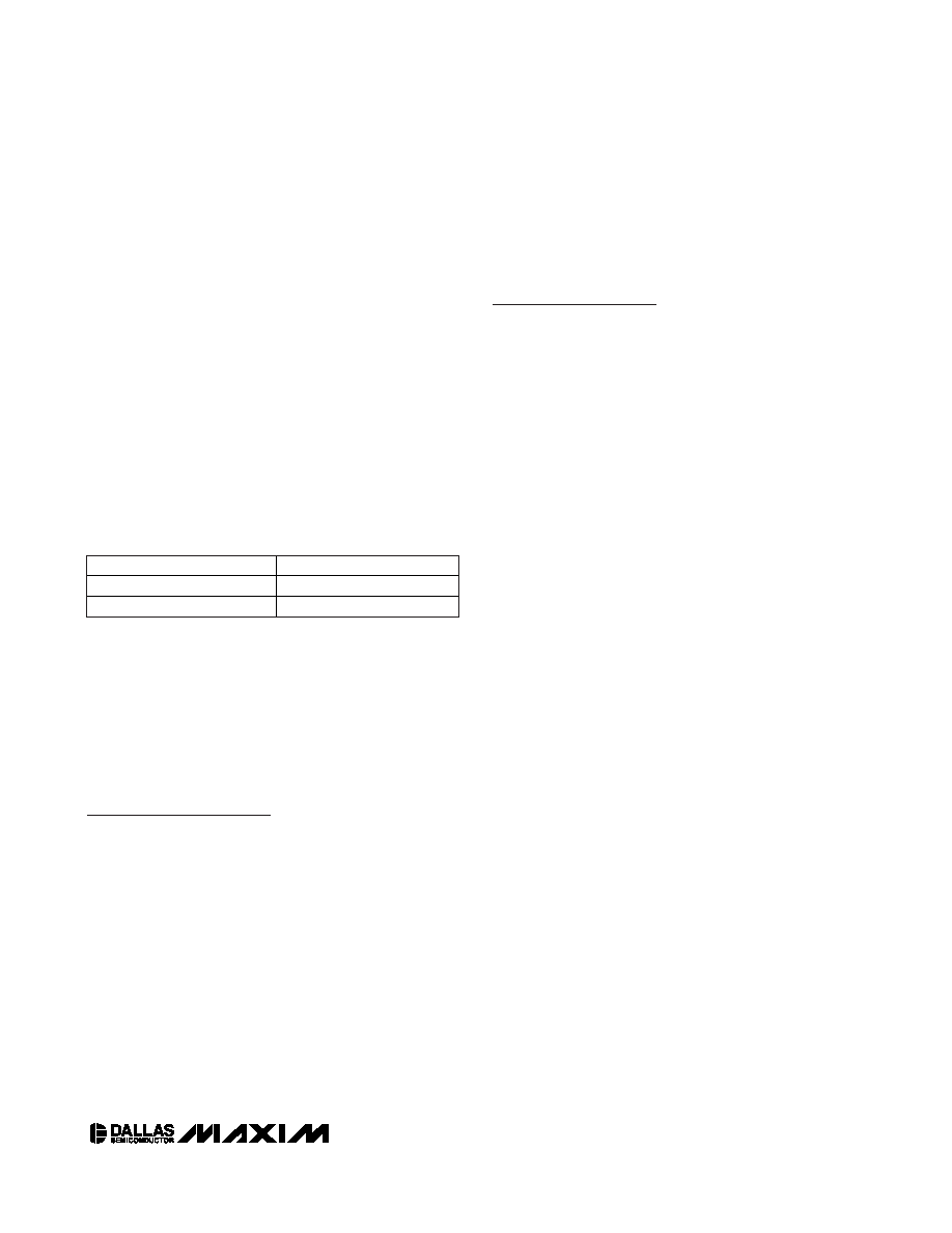
DEVICE
SLAVE ADDRESS
DS32B35
1010 A10A9A8R
DS32C35
1010 000R
R = Read/write select bit
Table 2. Memory Slave Address
相关PDF资料 |
PDF描述 |
|---|---|
| AD5259BCPZ10-R7 | IC POT DGTL 10K 256POS 10LFCSP |
| DS32B35-33# | IC RTC W/TCXO 20-SOIC |
| MS3112E22-41S | CONN RCPT 41POS BOX MNT W/SCKT |
| MS27473T22B21SC | CONN PLUG 21POS STRAIGHT W/SCKT |
| AD5248BRMZ100-RL7 | IC POT DGTL DUAL 100K I2C 10MSOP |
相关代理商/技术参数 |
参数描述 |
|---|---|
| DS32C35-33# | 功能描述:实时时钟 w/Integrated TCXO/Crystal/FRAM RoHS:否 制造商:Microchip Technology 功能:Clock, Calendar. Alarm RTC 总线接口:I2C 日期格式:DW:DM:M:Y 时间格式:HH:MM:SS RTC 存储容量:64 B 电源电压-最大:5.5 V 电源电压-最小:1.8 V 最大工作温度:+ 85 C 最小工作温度: 安装风格:Through Hole 封装 / 箱体:PDIP-8 封装:Tube |
| DS32C35-33#T&R | 制造商:Maxim Integrated Products 功能描述:IC RTC ACCURATE I2C 3.3V 20-SOIC |
| DS32C35-33#T&R | 功能描述:实时时钟 w/Integrated TCXO/Crystal/FRAM RoHS:否 制造商:Microchip Technology 功能:Clock, Calendar. Alarm RTC 总线接口:I2C 日期格式:DW:DM:M:Y 时间格式:HH:MM:SS RTC 存储容量:64 B 电源电压-最大:5.5 V 电源电压-最小:1.8 V 最大工作温度:+ 85 C 最小工作温度: 安装风格:Through Hole 封装 / 箱体:PDIP-8 封装:Tube |
| DS32C35-33IND | 制造商:MAXIM 制造商全称:Maxim Integrated Products 功能描述:Accurate I2C RTC with Integrated TCXO/Crystal/FRAM |
| DS32C35-33IND# | 功能描述:实时时钟 w/Integrated TCXO/Crystal/FRAM RoHS:否 制造商:Microchip Technology 功能:Clock, Calendar. Alarm RTC 总线接口:I2C 日期格式:DW:DM:M:Y 时间格式:HH:MM:SS RTC 存储容量:64 B 电源电压-最大:5.5 V 电源电压-最小:1.8 V 最大工作温度:+ 85 C 最小工作温度: 安装风格:Through Hole 封装 / 箱体:PDIP-8 封装:Tube |
发布紧急采购,3分钟左右您将得到回复。