- 您现在的位置:买卖IC网 > PDF目录9397 > DS3930E+ (Maxim Integrated Products)IC POT NV HEX I/O MEM 20-TSSOP PDF资料下载
参数资料
| 型号: | DS3930E+ |
| 厂商: | Maxim Integrated Products |
| 文件页数: | 2/12页 |
| 文件大小: | 0K |
| 描述: | IC POT NV HEX I/O MEM 20-TSSOP |
| 产品培训模块: | Lead (SnPb) Finish for COTS Obsolescence Mitigation Program |
| 标准包装: | 74 |
| 接片: | 256 |
| 电阻(欧姆): | 16.5k |
| 电路数: | 6 |
| 温度系数: | 标准值 ±250 ppm/°C |
| 存储器类型: | 非易失 |
| 接口: | I²C(设备位址) |
| 电源电压: | 2.7 V ~ 5.5 V |
| 工作温度: | -40°C ~ 85°C |
| 安装类型: | 表面贴装 |
| 封装/外壳: | 20-TSSOP(0.173",4.40mm 宽) |
| 供应商设备封装: | 20-TSSOP |
| 包装: | 管件 |
| 产品目录页面: | 1431 (CN2011-ZH PDF) |
DS3930
Hex Nonvolatile Potentiometer with
I/O and Memory
10
_____________________________________________________________________
terminated with a stop condition. The number of data
bytes transferred between start and stop conditions is
not limited and is determined by the master device. The
information is transferred byte-wise and each receiver
acknowledges with a ninth bit.
Within the bus specifications, a regular mode (100kHz
clock rate) and a fast mode (400kHz clock rate) are
defined. The DS3930 works in both modes.
Acknowledge: Each receiving device, when addressed,
is obliged to generate an acknowledge after the byte has
been received. The master device must generate an
extra clock pulse that is associated with this acknowl-
edge bit.
A device that acknowledges must pull down the SDA
line during the acknowledge clock pulse in such a way
that the SDA line is a stable low during the high period
of the acknowledge-related clock pulse. Of course,
setup and hold times must be taken into account. A
master must signal an end of data to the slave by not
generating an acknowledge bit on the last byte that has
been clocked out of the slave. In this case, the slave
must leave the data line high to enable the master to
generate the stop condition.
Data transfer from a master transmitter to a slave
receiver. The first byte transmitted by the master is the
command/control byte. Next follows a number of data
bytes. The slave returns an acknowledge bit after each
received byte.
Data transfer from a slave transmitter to a master
receiver. The master transmits the first byte (the com-
mand/control byte) to the slave. The slave then returns
an acknowledge bit. Next follows a number of data
bytes transmitted by the slave to the master. The mas-
ter returns an acknowledge bit after all received bytes
other than the last byte. At the end of the last received
byte, a not acknowledge can be returned.
The master device generates all serial clock pulses and
the start and stop conditions. A transfer is ended with a
stop condition or with a repeated start condition. Since
a repeated start condition is also the beginning of the
next serial transfer, the bus is not released.
The DS3930 can operate in the following three modes:
1)
Slave Receiver Mode: Serial data and clock are
received through SDA and SCL, respectively. After
each byte is received, an acknowledge bit is trans-
mitted. Start and stop conditions are recognized as
the beginning and end of a serial transfer. Address
recognition is performed by hardware after the
slave (device) address and direction bit have been
received.
2)
Slave Transmitter Mode: The first byte is received
and handled as in the slave receiver mode.
However, in this mode the direction bit indicates
that the transfer direction is reversed. Serial data is
transmitted on SDA by the DS3930 while the serial
clock is input on SCL. Start and stop conditions are
recognized as the beginning and end of a serial
transfer.
3)
Slave Address: This is the first byte received fol-
lowing the start condition from the master device.
The slave address consists of a 4-bit control code.
For the DS3930, this is set as 1010 binary for
read/write operations. The next bits of the slave
address are the device address (A2–A0). The last
bit of the slave address (R/W) defines the operation
to be performed. When set to a ‘1,’ a read operation
is selected, and when set to a ‘0,’ a write operation
is selected (see Figure 4).
Following the start condition, the DS3930 monitors the
SDA bus checking the device type identifier being
transmitted. Upon receiving the 1010 device identifier,
the appropriate device address bit, and the read/write
bit, the slave device outputs an acknowledge signal on
the SDA line.
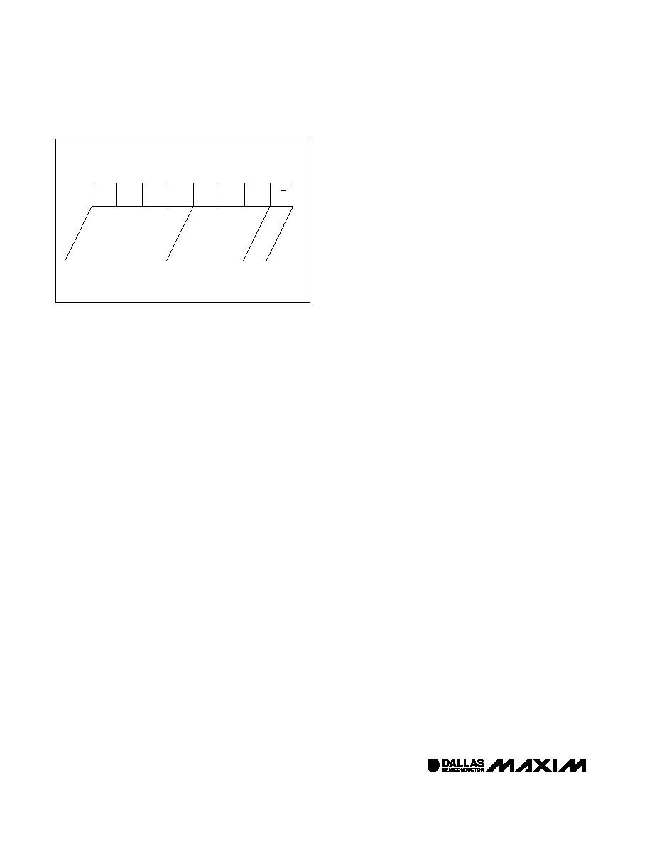
MSB
DEVICE
IDENTIFIER
DEVICE
ADDRESS
READ/WRITE
BIT
1
010
A2
A1
A0
R/W
LSB
Figure 4. Slave Address
相关PDF资料 |
PDF描述 |
|---|---|
| MAX5484ETE+ | IC POT DGTL 10BIT NV 16-TQFN |
| X1228S14IZ | IC RTC/CAL/SUP/ALRM 4K EE 14SOIC |
| MAX5483EUD+ | IC DGTL POT 10BIT NV 14-TSSOP |
| VI-JTM-MZ | CONVERTER MOD DC/DC 10V 25W |
| MAX5481EUD+ | IC DGTL POT 10BIT NV 14-TSSOP |
相关代理商/技术参数 |
参数描述 |
|---|---|
| DS3930E/T&R | 制造商:Maxim Integrated Products 功能描述:HEX NV POT WITH I/O & MEM T&R - Tape and Reel |
| DS3930E/T&R | 功能描述:数字电位计 IC RoHS:否 制造商:Maxim Integrated 电阻:200 Ohms 温度系数:35 PPM / C 容差:25 % POT 数量:Dual 每 POT 分接头:256 弧刷存储器:Volatile 缓冲刷: 数字接口:Serial (3-Wire, SPI) 描述/功能:Dual Volatile Low Voltage Linear Taper Digital Potentiometer 工作电源电压:1.7 V to 5.5 V 电源电流:27 uA 最大工作温度:+ 125 C 安装风格:SMD/SMT 封装 / 箱体:TQFN-16 封装:Reel |
| DS3930E+ | 功能描述:数字电位计 IC Hex Nonvolatile w/I/O & Memory RoHS:否 制造商:Maxim Integrated 电阻:200 Ohms 温度系数:35 PPM / C 容差:25 % POT 数量:Dual 每 POT 分接头:256 弧刷存储器:Volatile 缓冲刷: 数字接口:Serial (3-Wire, SPI) 描述/功能:Dual Volatile Low Voltage Linear Taper Digital Potentiometer 工作电源电压:1.7 V to 5.5 V 电源电流:27 uA 最大工作温度:+ 125 C 安装风格:SMD/SMT 封装 / 箱体:TQFN-16 封装:Reel |
| DS3930E+T&R | 制造商:Maxim Integrated Products 功能描述: 制造商:Maxim Integrated Products 功能描述:DGTL POTENTIOMETER 256POS 16.5KOHM HEX 20TSSOP - Tape and Reel 制造商:Maxim Integrated Products 功能描述:IC POT NV HEX I/O MEM 20-TSSOP 制造商:Maxim Integrated Products 功能描述:Digital Potentiometer ICs Hex Nonvolatile w/I/O & Memory |
| DS3930E+T&R | 功能描述:数字电位计 IC Hex Nonvolatile w/I/O & Memory RoHS:否 制造商:Maxim Integrated 电阻:200 Ohms 温度系数:35 PPM / C 容差:25 % POT 数量:Dual 每 POT 分接头:256 弧刷存储器:Volatile 缓冲刷: 数字接口:Serial (3-Wire, SPI) 描述/功能:Dual Volatile Low Voltage Linear Taper Digital Potentiometer 工作电源电压:1.7 V to 5.5 V 电源电流:27 uA 最大工作温度:+ 125 C 安装风格:SMD/SMT 封装 / 箱体:TQFN-16 封装:Reel |
发布紧急采购,3分钟左右您将得到回复。