- 您现在的位置:买卖IC网 > PDF目录9434 > DS4000CWN/WBGA (Maxim Integrated Products)IC OSC TCXO 12.8MHZ 24-BGA PDF资料下载
参数资料
| 型号: | DS4000CWN/WBGA |
| 厂商: | Maxim Integrated Products |
| 文件页数: | 5/16页 |
| 文件大小: | 0K |
| 描述: | IC OSC TCXO 12.8MHZ 24-BGA |
| 标准包装: | 1 |
| 类型: | 温度 - 补偿晶体振荡器(TCXO) |
| 频率: | 12.8MHz |
| 电源电压: | 4.75 V ~ 5.25 V |
| 电流 - 电源: | 1.5mA |
| 工作温度: | -40°C ~ 85°C |
| 封装/外壳: | 24-BBGA |
| 包装: | 托盘 |
| 供应商设备封装: | 24-WBGA(11x9) |
| 安装类型: | 表面贴装 |
DS4000 Digitally Controlled TCXO
13 of 16
SLAVE ADDRESS
The slave address is the first byte received following the START condition generated by the master device. The
address byte consists of a 7-bit slave address and the R/
W direction bit. The DS4000 slave address is set to
100010A0, where A0 is externally hardwired to a HIGH or LOW state. This allows design flexibility to set the slave’s
address to one of two possible address locations. The last bit following the slave address is the direction bit (R/
W)
and defines the operation to be performed by the master, transmit data (R/
W = 0), or receive data (R/W = 1).
Following the START condition, the DS4000 monitors the SDA bus by checking the slave address being
transmitted. Upon receiving the proper slave address and R/
W bit, the slave device outputs an acknowledge signal
on the SDA line regardless of the operation mode.
The DS4000 can operate in the following two modes:
1) Slave Receiver Mode: Serial data and clock are received through SDA and SCL. After each byte is received,
an acknowledge bit is transmitted. START and STOP conditions are recognized as the beginning and end of a
serial transfer. Address recognition is performed by the hardware after reception of the slave address and
direction bit (Figure 4).
2) Slave Transmitter Mode: The first byte is received and handled as in the slave receiver mode. However, in
this mode, the direction bit indicates that the transfer direction is reversed. Serial data is transmitted on SDA by
the DS4000 while the serial clock is input on SCL. START and STOP conditions are recognized as the
beginning and end of a serial transfer (Figure 5).
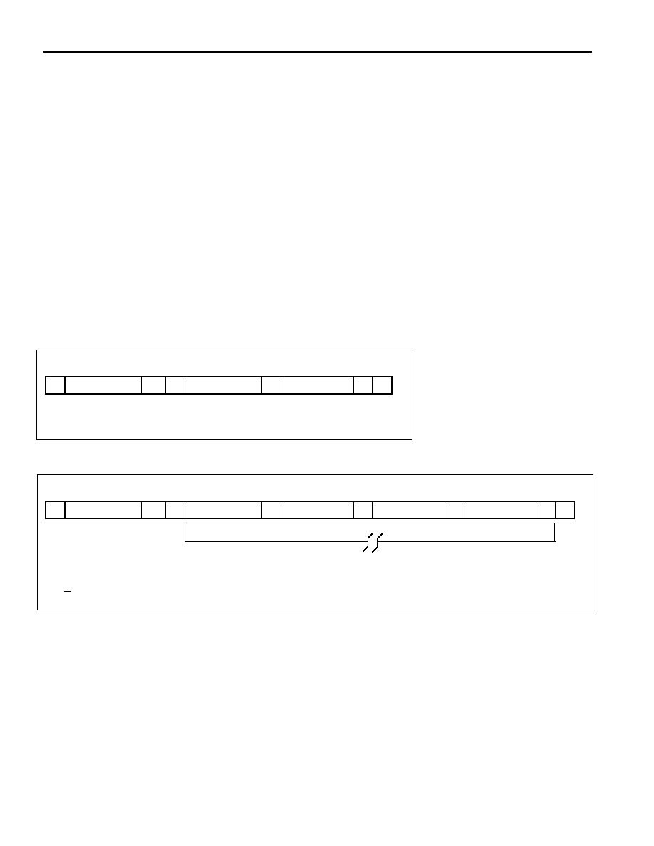
Figure 4. Data Write—Slave Receiver Mode
<SLAVE ADDRESS>
R/
W
<DATA ADDRESS>
<DATA (n)>
S
100010A0
0
A
XXXXXXXX
A
XXXXXXXX
A P
S = START
A = ACKNOWLEDGE
P = STOP
Figure 5. Data Read—Slave Transmitter Mode
<SLAVE ADDRESS>
R/W
<DATA (n)>
<DATA (n + 1)>
<DATA (n + 2)>
<DATA (n + X)>
S
100010A0
1
A
XXXXXXXX
A
XXXXXXXX
A
XXXXXXXX
A
XXXXXXXX
A P
S = START
A = ACKNOWLEDGE
P = STOP
A = NOT ACKNOWLEDGE
相关PDF资料 |
PDF描述 |
|---|---|
| MS3451W20-14P | CONN RCPT 5POS CBL MNT W/PINS |
| MS3451L20-14PZ | CONN RCPT 5POS CBL MNT W/PINS |
| AD5247BKSZ10-RL7 | IC POT DGTL 10K 128POS SC70-6 |
| DS4000A0/WBGA | IC OSC TCXO 10MHZ 24BGA |
| MS3451L20-14PY | CONN RCPT 5POS CBL MNT W/PINS |
相关代理商/技术参数 |
参数描述 |
|---|---|
| DS4000D0/WBGA | 功能描述:IC OSC TCXO 13MHZ 24-BGA RoHS:否 类别:集成电路 (IC) >> 时钟/计时 - 可编程计时器和振荡器 系列:- 产品培训模块:Lead (SnPb) Finish for COTS Obsolescence Mitigation Program 标准包装:45 系列:- 类型:温度 - 补偿晶体振荡器(TCXO) 计数:- 频率:25MHz 电源电压:3.135 V ~ 3.465 V 电流 - 电源:1.5mA 工作温度:-40°C ~ 85°C 封装/外壳:16-SOIC(0.295",7.50mm 宽) 包装:管件 供应商设备封装:16-SOIC W 安装类型:表面贴装 |
| DS4000D0N/WBGA | 功能描述:IC OSC TCXO 13MHZ 24-BGA RoHS:否 类别:集成电路 (IC) >> 时钟/计时 - 可编程计时器和振荡器 系列:- 产品培训模块:Lead (SnPb) Finish for COTS Obsolescence Mitigation Program 标准包装:45 系列:- 类型:温度 - 补偿晶体振荡器(TCXO) 计数:- 频率:25MHz 电源电压:3.135 V ~ 3.465 V 电流 - 电源:1.5mA 工作温度:-40°C ~ 85°C 封装/外壳:16-SOIC(0.295",7.50mm 宽) 包装:管件 供应商设备封装:16-SOIC W 安装类型:表面贴装 |
| DS4000EC/WBGA | 功能描述:IC OSC TCXO 14.31818MHZ 24-BGA RoHS:否 类别:集成电路 (IC) >> 时钟/计时 - 可编程计时器和振荡器 系列:- 产品培训模块:Lead (SnPb) Finish for COTS Obsolescence Mitigation Program 标准包装:45 系列:- 类型:温度 - 补偿晶体振荡器(TCXO) 计数:- 频率:25MHz 电源电压:3.135 V ~ 3.465 V 电流 - 电源:1.5mA 工作温度:-40°C ~ 85°C 封装/外壳:16-SOIC(0.295",7.50mm 宽) 包装:管件 供应商设备封装:16-SOIC W 安装类型:表面贴装 |
| DS4000ECN/WBGA | 功能描述:IC OSC TCXO 14.31818MHZ 24-BGA RoHS:否 类别:集成电路 (IC) >> 时钟/计时 - 可编程计时器和振荡器 系列:- 产品培训模块:Lead (SnPb) Finish for COTS Obsolescence Mitigation Program 标准包装:45 系列:- 类型:温度 - 补偿晶体振荡器(TCXO) 计数:- 频率:25MHz 电源电压:3.135 V ~ 3.465 V 电流 - 电源:1.5mA 工作温度:-40°C ~ 85°C 封装/外壳:16-SOIC(0.295",7.50mm 宽) 包装:管件 供应商设备封装:16-SOIC W 安装类型:表面贴装 |
| DS4000G0/WBGA | 功能描述:TCXO振荡器 RoHS:否 制造商:AVX 封装 / 箱体: 频率:32.768 kHz 频率稳定性: 负载电容:15 pF 端接类型:SMD/SMT 电源电压:3 V 尺寸:2.5 mm W x 3.2 mm L x 1 mm H 输出格式:CMOS 最小工作温度:- 40 C 最大工作温度:+ 85 C 封装:Reel |
发布紧急采购,3分钟左右您将得到回复。