参数资料
| 型号: | DS4026S+JCN |
| 厂商: | Maxim Integrated Products |
| 文件页数: | 2/14页 |
| 文件大小: | 0K |
| 描述: | IC OSC TCXO 20MHZ 16-SOIC |
| 产品培训模块: | Lead (SnPb) Finish for COTS Obsolescence Mitigation Program |
| 标准包装: | 45 |
| 类型: | 温度 - 补偿晶体振荡器(TCXO) |
| 频率: | 20MHz |
| 电源电压: | 3.135 V ~ 3.465 V |
| 电流 - 电源: | 1.5mA |
| 工作温度: | -40°C ~ 85°C |
| 封装/外壳: | 16-SOIC(0.295",7.50mm 宽) |
| 包装: | 管件 |
| 供应商设备封装: | 16-SOIC W |
| 安装类型: | 表面贴装 |
| 产品目录页面: | 1434 (CN2011-ZH PDF) |
DS4026
10MHz to 51.84MHz TCXO
10
______________________________________________________________________________________
Read Mode
In the temperature register (see the
Temperature
Register (02h–03h) table), temperature is represented
as a 12-bit code and is accessible at location 02h and
03h. The upper 8 bits are at location 02h and the lower
4 bits are in the upper nibble of the byte at location
03h. Upon power reset, the registers are set to a +25°C
default temperature and the controller starts a tempera-
ture conversion. The temperature register stores new
temperature readings.
The current temperature is loaded into the (user) tem-
perature registers when a valid I2C slave address and
write is received and when a word address is received.
Consequently, if the two temperature registers are read
in individual I2C transactions, it is possible for a tem-
perature conversion to occur between reads, and the
results can be inaccurate. To prevent this from occur-
ring, the registers should be read using a single, multi-
byte read operation (Figure 5). I2C reads do not affect
the internal temperature registers.
I2C Serial Data Bus
The DS4026 supports a bidirectional I2C bus and data
transmission protocol. A device that sends data onto
the bus is defined as a transmitter and a device receiv-
ing data is defined as a receiver. The device that con-
trols the message is called a master. The devices that
are controlled by the master are slaves. The bus must
be controlled by a master device that generates the
serial clock (SCL), controls the bus access, and gener-
ates the START and STOP conditions. The DS4026
operates as a slave on the I2C bus. Connections to the
bus are made through the open-drain I/O lines SDA
and SCL. Within the bus specifications, a standard
mode (100kHz maximum clock rate) and a fast mode
(400kHz maximum clock rate) are defined. The DS4026
works in both modes.
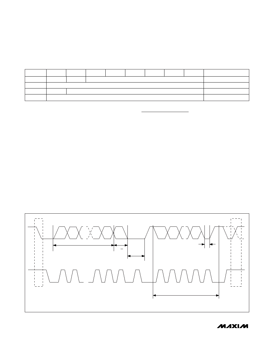
The following bus protocol has been defined (Figure 3):
Data transfer can be initiated only when the bus is
not busy.
Table 1. Register Map
ADDRESS
BIT 7
BIT 6
BIT 5
BIT 4
BIT 3
BIT 2
BIT 1
BIT 0
FUNCTION
00
DCOMP
SIGN
FTUNEH
Frequency Tuning High
01
FTUNEL
Frequency Tuning Low
02
SIGN
TREGH
Temperature MSB
03
TREGL
Temperature LSB
STOP
CONDITION
OR REPEATED
START
CONDITION
REPEATED IF MORE BYTES
ARE TRANSFERED
ACK
START
CONDITION
ACK
ACKNOWLEDGEMENT
SIGNAL FROM RECEIVER
ACKNOWLEDGEMENT
SIGNAL FROM RECEIVER
SLAVE ADDRESS
MSB
SCL
SDA
R/W
DIRECTION
BIT
12
6
7
8
9
1
2
8
9
3–7
Figure 3. I2C Data Transfer Overview
相关PDF资料 |
PDF描述 |
|---|---|
| V375B12M300BG3 | CONVERTER MOD DC/DC 12V 300W |
| LTC1093CN#PBF | IC DATA ACQ SYS 10BIT 6CH 16-DIP |
| DS4M200D+33 | IC OSC CLOCK 200MHZ 10-LCCC |
| DS4250D+ | IC OSC CLOCK 250MHZ 10-LCCC |
| LTC1093CN | IC DATA ACQ SYS 10BIT 6CH 16-DIP |
相关代理商/技术参数 |
参数描述 |
|---|---|
| DS4026S-PCNEVKIT | 功能描述:时钟和定时器开发工具 RoHS:否 制造商:Texas Instruments 产品:Evaluation Modules 类型:Clock Conditioners 工具用于评估:LMK04100B 频率:122.8 MHz 工作电源电压:3.3 V |
| DS4026S-QCC | 功能描述:TCXO振荡器 RoHS:否 制造商:AVX 封装 / 箱体: 频率:32.768 kHz 频率稳定性: 负载电容:15 pF 端接类型:SMD/SMT 电源电压:3 V 尺寸:2.5 mm W x 3.2 mm L x 1 mm H 输出格式:CMOS 最小工作温度:- 40 C 最大工作温度:+ 85 C 封装:Reel |
| DS4026S-QCN | 功能描述:TCXO振荡器 RoHS:否 制造商:AVX 封装 / 箱体: 频率:32.768 kHz 频率稳定性: 负载电容:15 pF 端接类型:SMD/SMT 电源电压:3 V 尺寸:2.5 mm W x 3.2 mm L x 1 mm H 输出格式:CMOS 最小工作温度:- 40 C 最大工作温度:+ 85 C 封装:Reel |
| DS4-02P | 制造商:Cooper Bussmann 功能描述:TOP SCREW-ON INSERTION BRIDGE, 2 POLE, F - Bulk 制造商:COOPER BUSSMANN 功能描述:TOP SCREW-ON INSERTION BRIDGE, 2 POLE, F |
| DS402ST | 制造商:DYNEX 制造商全称:Dynex Semiconductor 功能描述:Rectifier Diode |
发布紧急采购,3分钟左右您将得到回复。