- 您现在的位置:买卖IC网 > PDF目录2146 > DS4420N+T&R (Maxim Integrated Products)IC AMP AUDIO MONO AB DIFF 14TDFN PDF资料下载
参数资料
| 型号: | DS4420N+T&R |
| 厂商: | Maxim Integrated Products |
| 文件页数: | 3/10页 |
| 文件大小: | 0K |
| 描述: | IC AMP AUDIO MONO AB DIFF 14TDFN |
| 产品培训模块: | Lead (SnPb) Finish for COTS Obsolescence Mitigation Program |
| 标准包装: | 2,500 |
| 放大器类型: | 音频 |
| 电路数: | 1 |
| 输出类型: | 差分 |
| 电流 - 电源: | 1.7mA |
| 电流 - 输出 / 通道: | 95mA |
| 电压 - 电源,单路/双路(±): | 4.5 V ~ 5.5 V |
| 工作温度: | -20°C ~ 70°C |
| 安装类型: | 表面贴装 |
| 封装/外壳: | 14-WFDFN 裸露焊盘 |
| 供应商设备封装: | 14-TDFN-EP(3x3) |
| 包装: | 带卷 (TR) |
DS4420
I2C Programmable-Gain Amplifier
for Audio Applications
2
_____________________________________________________________________
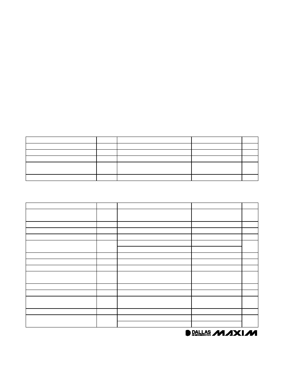
ABSOLUTE MAXIMUM RATINGS
RECOMMENDED OPERATING CONDITIONS
(TA = -20°C to +70°C.)
Stresses beyond those listed under “Absolute Maximum Ratings” may cause permanent damage to the device. These are stress ratings only, and functional
operation of the device at these or any other conditions beyond those indicated in the operational sections of the specifications is not implied. Exposure to
absolute maximum rating conditions for extended periods may affect device reliability.
Voltage on VCC, SDA, and SCL
Relative to GND.................................................-0.5V to +6.0V
Voltage on A0, A1, and A2
Relative to GND ......................................-0.5V to (VCC + 0.5V;
not to exceed 6.0V)
Voltage on IN+, IN-, OUT-, and OUT+
Relative to AGND .................................-0.5V to (AVCC + 0.5V;
not to exceed 6.0V)
Voltage on AVCC Relative to VCC..........................-0.3V to +0.3V
Voltage on AGND Relative to GND .......................-0.3V to +0.3V
Output Current ..................................................................150mA
Operating Temperature Range ...........................-20°C to +70°C
Storage Temperature .....................See J-STD-020 Specification
PARAMETER
SYMBOL
CONDITIONS
MIN
TYP
MAX
UNITS
Digital Supply Voltage
VCC
(Note 1)
+4.5
+5.5
V
Analog Supply Voltage
AVCC
VCC
V
Analog Ground
AGND
(See Figure 5)
GND
V
Input Logic 1 (SCL, SDA, A0, A1, A2)
VIH
2.0
VCC
+ 0.3
V
Input Logic 0 (SCL, SDA, A0, A1, A2)
VIL
-0.3
+0.8
V
ELECTRICAL CHARACTERISTICS
(VCC = +4.5V to +5.5V, TA = -20°C to +70°C, unless otherwise noted.)
PARAMETER
SYMBOL
CONDITIONS
MIN
TYP
MAX
UNITS
Supply Current
ICC
VCC = 5.5V, RL = ∞, VIN = 0V differential
(Note 9)
1.7
3
mA
Standby Current
ISTBY
VCC = 5.5V (Notes 2, 9)
140
A
Input Leakage (SDA, SCL, A2, A1, A0)
IIL
VCC = 5.5V
1
A
Output Leakage (SDA)
IL
1A
VOL = 0.4V
3
Output-Current Low (SDA)
IOL
VOL = 0.6V
6
mA
Input Voltage Range
VIN
Differential
-19
+1
dBV
Max Peak-to-Peak Input Level
VINP-P
Differential
3.2
V
Input Resistance
RIN
Differential, active mode (Note 3)
29
49
60
kΩ
Input Common-Mode Voltage
VIN:CM
0.45 x
VCC
0.55 x
VCC
V
Output Voltage
VO
RL = 50Ω differential
6
dBV
Output Peak-to-Peak Signal Swing
VOP-P
Differential
5.6
V
Output Common-Mode Voltage
VO:CM
0.45 x
VCC
0.5 x
VCC
0.55 x
VCC
V
Output Offset Voltage
VO:OS
AV = +25dB
-20
+20
mV
VOUT = GND
95
Amplifier Output Current
(Sourcing)
IOS1
VOUT = VCC - 0.75V
64
mA
相关PDF资料 |
PDF描述 |
|---|---|
| DUM-5246L-R | MIC CONDENSER ELECT UNI -46DB |
| DV-T263-101E | HEATSINK FOR TO-263 |
| DV4112/2NP-30201 | FAN TUBEAXIAL 119X38MM 12VDC |
| DV4114N | FAN 119X38MM 24VDC 161.9CFM |
| DV4118N | FAN 119X38MM 48VDC 161.9CFM |
相关代理商/技术参数 |
参数描述 |
|---|---|
| DS4421FP000 | 制造商:Thomas & Betts 功能描述:400A,CON,3P4W,MG,421,3P440V |
| DS4421MP000 | 制造商:Thomas & Betts 功能描述:400A,PLG,3P4W,MG,421,3P440V |
| DS4421MR000 | 制造商:Thomas & Betts 功能描述:400A,NLT,3P4W,MG,421,3P440V |
| DS4422 | 制造商:MAXIM 制造商全称:Maxim Integrated Products 功能描述:Two-/Four-Channel, I2C, 7-Bit Sink/Source Current DAC |
| DS4422_09 | 制造商:MAXIM 制造商全称:Maxim Integrated Products 功能描述:Two-/Four-Channel, I2C, 7-Bit Sink/Source Current DAC |
发布紧急采购,3分钟左右您将得到回复。