- 您现在的位置:买卖IC网 > PDF目录223667 > DS75361N (NATIONAL SEMICONDUCTOR CORP) Dual TTL-to-MOS Driver PDF资料下载
参数资料
| 型号: | DS75361N |
| 厂商: | NATIONAL SEMICONDUCTOR CORP |
| 元件分类: | 门电路 |
| 英文描述: | Dual TTL-to-MOS Driver |
| 中文描述: | TTL/H/L SERIES, DUAL 1-INPUT NAND GATE, PDIP8 |
| 封装: | PLASTIC, DIP-8 |
| 文件页数: | 5/6页 |
| 文件大小: | 353K |
| 代理商: | DS75361N |
Typical Applications
The fast switching speeds of this device may produce unde-
sirable output transient overshoot because of load or wiring
inductance A small series damping resistor may be used to
reduce or eliminate this output transient overshoot The
optimum value of the damping resistor to use depends on
the specific load characteristics and switching speed A typi-
cal value would be between 10X and 30X
(Figure 3)
TLF7557 – 6
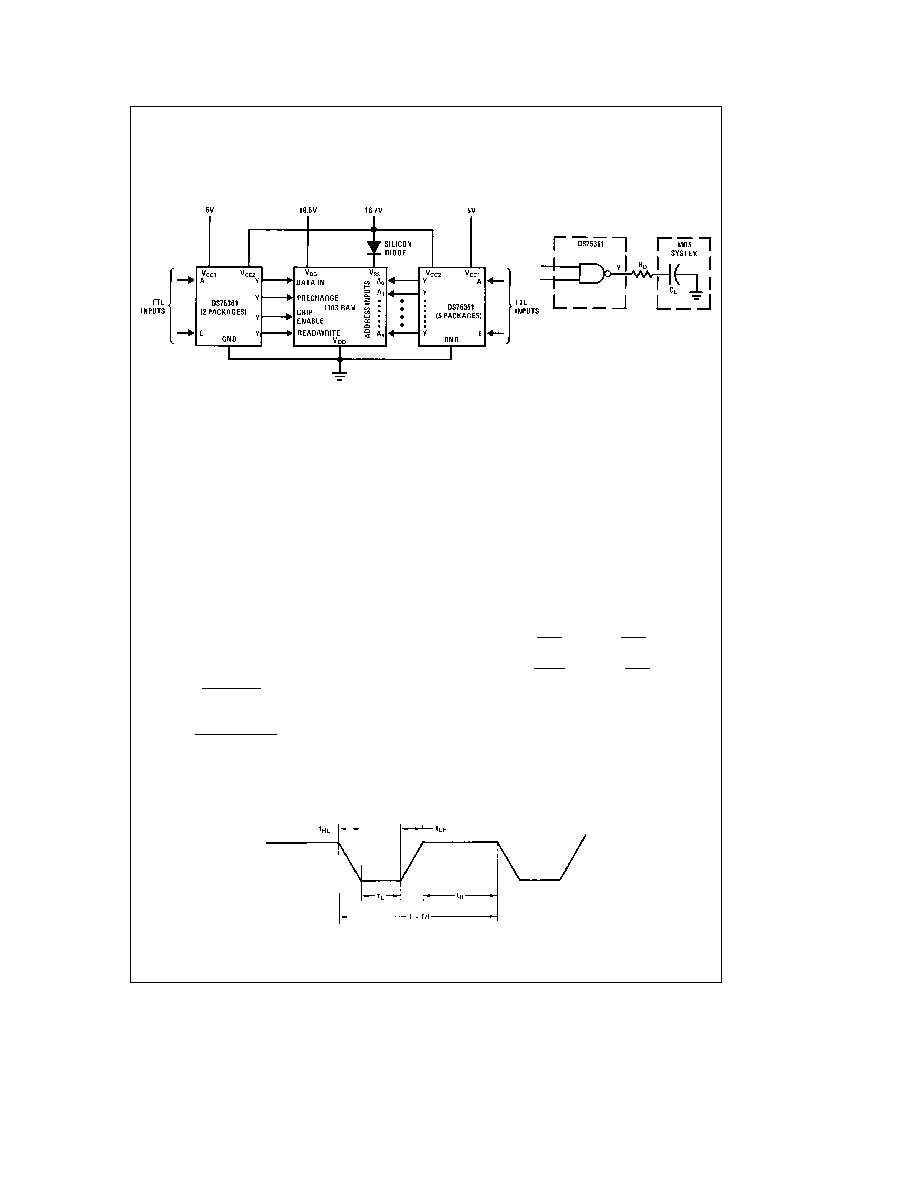
FIGURE 2 Interconnection of DS75361 Devices with 1103 RAM
TLF7557 – 7
Note
RD
10X to 30X (Optional)
FIGURE 3 Use of Damping
Resistor to Reduce or Eliminate
Output Transient Overshoot in
Certain DS75361 Applications
Thermal Information
POWER DISSIPATION PRECAUTIONS
Significant power may be dissipated in the DS75361 driver
when charging and discharging high-capacitance loads over
a wide voltage range at high frequencies The total dissipa-
tion curve shows the power dissipated in a typical DS75361
as a function of load capacitance and frequency Average
power dissipated by this driver can be broken into three
components
PT(AV) e PDC(AV) a PC(AV) a PS(AV)
where PDC(AV) is the steady-state power dissipation with the
output high or low PC(AV) is the power level during charging
or discharging of the load capacitance and PS(AV) is the
power dissipation during switching between the low and
high levels None of these include energy transferred to the
load and all are averaged over a full cycle
The power components per driver channel are
PDC(AV) e
PLtL a PHtH
T
PC(AV)
CVC2 f
PS(AV) e
PLHtLH a PHLtHL
T
where the times are defined in
Figure 4
PL PH PLH and PHL are the respective instantaneous lev-
els of power dissipation and C is load capacitance
The DS75361 is so designed that PS is a negligible portion
of PT in most applications Except at very high frequencies
tL a tH n tLH a tHL so that PS can be neglected The total
dissipation curve for no load demonstrates this point The
power dissipation contributions from both channels are then
added together to obtain total device power
The following example illustrates this power calculation
technique Assume both channels are operating identically
with C e 200 pF f e 2 MHz VCC1 e 5V VCC2 e 20V and
duty cycle e 60% outputs high (tH T e 06) Also assume
VOH e 193V VOL e 01V PS is negligible and that the
current from VCC2 is negligible when the output is high
On a per-channel basis using data sheet values
PDC(AV) e
(5V)
2mA2J a(20V) 0mA2J( (06)a
(5V)
16mA
2
J a(20V) 7mA2J( (04)
PDC(AV) e 47 mW per channel
PC(AV)
(200 pF) (192V)2 (2 MHz)
PC(AV)
148 mW per channel
For the total device dissipation of the two channels
PT(AV)
2 (47 a 148)
PT(AV)
390 mW typical for total package
TLF7557 – 8
FIGURE 4 Output Voltage Waveform
5
Obsolete
相关PDF资料 |
PDF描述 |
|---|---|
| DS75361 | Dual TTL-to-MOS Driver |
| DSC-10510-193 | DIGITAL TO SYNCHRO OR RESOLVER, DMA40 |
| DSC-10510-163S | DIGITAL TO SYNCHRO OR RESOLVER, DMA40 |
| DSC5031-29HB | DIGITAL TO SYNCHRO OR RESOLVER, XMA26 |
| DSC5131-249SS | DIGITAL TO SYNCHRO OR RESOLVER, XMA26 |
相关代理商/技术参数 |
参数描述 |
|---|---|
| DS75361N/A+ | 制造商:未知厂家 制造商全称:未知厂家 功能描述:TTL-to-MOS Translator |
| DS75361N-8/A+ | 制造商:未知厂家 制造商全称:未知厂家 功能描述:TTL-to-MOS Translator |
| DS75361N-8/B+ | 制造商:未知厂家 制造商全称:未知厂家 功能描述:TTL-to-MOS Translator |
| DS75362J-8 | 制造商:未知厂家 制造商全称:未知厂家 功能描述:TTL-to-MOS Translator |
| DS75362J-8/A+ | 制造商:未知厂家 制造商全称:未知厂家 功能描述:TTL-to-MOS Translator |
发布紧急采购,3分钟左右您将得到回复。