参数资料
| 型号: | DS8102+ |
| 厂商: | Maxim Integrated Products |
| 文件页数: | 2/9页 |
| 文件大小: | 0K |
| 描述: | IC MODULATOR/DECODER 16-TSSOP |
| 产品培训模块: | Lead (SnPb) Finish for COTS Obsolescence Mitigation Program |
| 标准包装: | 96 |
| 类型: | 调制器 |
| 应用: | 电量测量 |
| 安装类型: | 表面贴装 |
| 封装/外壳: | 16-TSSOP(0.173",4.40mm 宽) |
| 供应商设备封装: | 16-TSSOP |
| 包装: | 管件 |
| 其它名称: | 90-08102+XPX |
DS8102
Dual Delta-Sigma Modulator and Encoder
2
_______________________________________________________________________________________
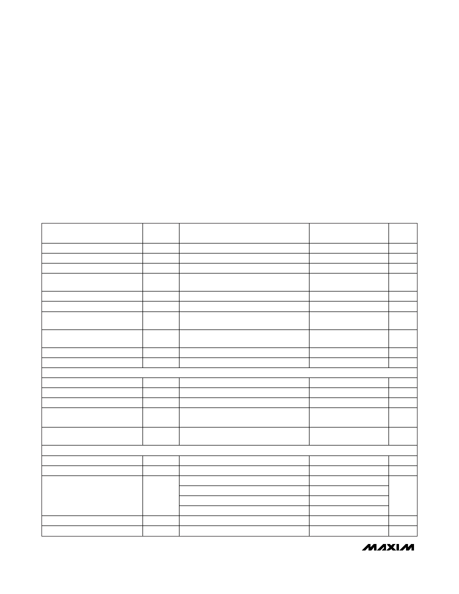
ABSOLUTE MAXIMUM RATINGS
ELECTRICAL CHARACTERISTICS
(VDD = 2.7V to 3.6V, TA = -40°C to +85°C, fCLK = 8MHz, VREF = internal, OSR = 128, unless otherwise noted.) (Note 1)
Stresses beyond those listed under “Absolute Maximum Ratings” may cause permanent damage to the device. These are stress ratings only, and functional
operation of the device at these or any other conditions beyond those indicated in the operational sections of the specifications is not implied. Exposure to
absolute maximum rating conditions for extended periods may affect device reliability.
Voltage Range on VDD Relative to DGND.............-0.3V to +4.0V
Voltage Range on VDD Relative to AGND .............-0.3V to +4.0V
Voltage Range on AGND Relative to DGND .........-0.3V to +0.3V
Voltage Range on Any Pin Relative to DGND
Except AN0+, AN0-, and AN1+, AN1- ...............-0.3V to +4.0V
Voltage Range on AN0+, AN0-, AN1+, and AN1-
Relative to AGND ...............................................-4.0V to +4.0V
Operating Temperature Range ...........................-40°C to +85°C
Storage Temperature Range .............................-65°C to +150°C
Soldering Temperature...........................Refer to the IPC/JEDEC
J-STD-020 Specification.
PARAMETER
SYMBOL
CONDITIONS
MIN
TYP
(Note 2)
MAX
UNITS
Supply Voltage
VDD
VRST
3.3
3.6
V
Power-Fail Reset Voltage
VRST
Monitors VDD
2.7
2.8
2.99
V
Active VDD Current
IDD
Normal operation
3.5
5.0
mA
Shutdown (Power-Down) VDD
Current
ISTOP
RST = 0 or VDD < VRST
2
nA
Input Low Voltage
VIL
DGND
0.3 x VDD
V
Input High Voltage
VIH
0.7 x VDD
VDD
V
Output Low Voltage
(CLKIO, MNOUT)
VOL
IOL = 4mA
DGND
0.4
V
Output High Voltage
(CLKIO, MNOUT)
VOH
IOH = -4mA
VDD - 0.4
V
Input/Output Pin Capacitance
CIO
(Note 3)
15
pF
Input Leakage Current (All Inputs)
IL
-100
+100
nA
CLOCK SOURCE
External Clock Input Frequency
fXCLK
CLKSEL = 1
DC
8
MHz
External Clock Input Period
tXCLK-CLCL CLKSEL = 1
125
ns
External Clock Input Duty Cycle
tXCLK-DUTY CLKSEL = 1
40
60
%
Internal Oscillator Output
Frequency
fICLK
CLKSEL = 0
7.5
8.0
8.5
MHz
Internal Oscillator Output Duty
Cycle
tICLK-DUTY
CLKSEL = 0
47.8
49.1
49.7
%
ANALOG-TO-DIGITAL CONVERTER
AFE Warmup Delay
tWU1
fICLK = 8MHz (Notes 1, 4)
1.02
ms
Reference Buffer Warmup Delay
tWU2
fICLK = 8MHz (Notes 1, 5)
7.17
ms
OSR = 32
16
OSR = 64
19
OSR = 128
22
Decimator Output (Note 6)
OSR = 256
24
Bits
Integral Nonlinearity
INL
(Notes 1, 6)
±0.01
%FSR
Offset Error
Gain = 1 (Note 6)
1.4
mV
相关PDF资料 |
PDF描述 |
|---|---|
| DS8113-JNG+ | IC INTERFACE SMART CARD 28-TSSOP |
| DS8313-RRX+ | IC INTERFACE SMART CARD 28-SOIC |
| DS8500-JND+T&R | IC MODEM HART SGL 3.6V 20-TQFN |
| DS87C520-ENL | IC MCU EPROM/ROM 33MH IND 44TQFP |
| DS87C530-ECL+ | IC MCU EPR/ROM W/RTC 33MZ 52TQFP |
相关代理商/技术参数 |
参数描述 |
|---|---|
| DS8102+ | 功能描述:编码器、解码器、复用器和解复用器 Dual Delta-Sigma Modulator & Encoder RoHS:否 制造商:Micrel 产品:Multiplexers 逻辑系列:CMOS 位数: 线路数量(输入/输出):2 / 12 传播延迟时间:350 ps, 400 ps 电源电压-最大:2.625 V, 3.6 V 电源电压-最小:2.375 V, 3 V 最大工作温度:+ 85 C 安装风格:SMD/SMT 封装 / 箱体:QFN-44 封装:Tray |
| DS811 | 制造商:未知厂家 制造商全称:未知厂家 功能描述:Analog IC |
| DS8113 | 制造商:MAXIM 制造商全称:Maxim Integrated Products 功能描述:Smart Card Interface |
| DS8113_10 | 制造商:MAXIM 制造商全称:Maxim Integrated Products 功能描述:Smart Card Interface |
| DS8113-JNG+ | 功能描述:接口 - 专用 Smart Card Interface RoHS:否 制造商:Texas Instruments 产品类型:1080p60 Image Sensor Receiver 工作电源电压:1.8 V 电源电流:89 mA 最大功率耗散: 最大工作温度:+ 85 C 安装风格:SMD/SMT 封装 / 箱体:BGA-59 |
发布紧急采购,3分钟左右您将得到回复。