- 您现在的位置:买卖IC网 > PDF目录10917 > DS89C430-MNL+ (Maxim Integrated Products)IC MCU FLASH 16KB 33MHZ 40-DIP PDF资料下载
参数资料
| 型号: | DS89C430-MNL+ |
| 厂商: | Maxim Integrated Products |
| 文件页数: | 22/46页 |
| 文件大小: | 0K |
| 描述: | IC MCU FLASH 16KB 33MHZ 40-DIP |
| 产品培训模块: | Lead (SnPb) Finish for COTS Obsolescence Mitigation Program |
| 标准包装: | 10 |
| 系列: | 89C |
| 核心处理器: | 8051 |
| 芯体尺寸: | 8-位 |
| 速度: | 33MHz |
| 连通性: | EBI/EMI,SIO,UART/USART |
| 外围设备: | 电源故障复位,WDT |
| 输入/输出数: | 32 |
| 程序存储器容量: | 16KB(16K x 8) |
| 程序存储器类型: | 闪存 |
| RAM 容量: | 1K x 8 |
| 电压 - 电源 (Vcc/Vdd): | 4.5 V ~ 5.5 V |
| 振荡器型: | 外部 |
| 工作温度: | -40°C ~ 85°C |
| 封装/外壳: | 40-DIP(0.600",15.24mm) |
| 包装: | 管件 |
第1页第2页第3页第4页第5页第6页第7页第8页第9页第10页第11页第12页第13页第14页第15页第16页第17页第18页第19页第20页第21页当前第22页第23页第24页第25页第26页第27页第28页第29页第30页第31页第32页第33页第34页第35页第36页第37页第38页第39页第40页第41页第42页第43页第44页第45页第46页
DS89C430/DS89C450 Ultra-High-Speed Flash Microcontrollers
29 of 46
Page Mode, External Memory Cycle
Page mode retains the basic circuitry requirement for an original 8051 external memory interface, but alters the
configuration of P0 and P2 for the purposes of address output and data I/O during external memory cycles.
Additionally, the functions of ALE and PSEN are altered to support this mode of operation.
Setting the PAGEE (ACON.7) bit to logic 1 enables page mode. Clearing the PAGEE bit to logic 0 disables the
page mode and the external bus structure defaults to the original 8051 expanded bus configuration (nonpage
mode). The DS89C430 supports page mode in two external bus structures. The logic value of the page-mode-
select bits in the ACON register determines the external bus structure and the basic memory cycle in number of
system clocks. Table 6 summarizes this option. The first three selections use the same bus structure but with
different memory cycle time. Setting the select bits to 11b selects another bus structure. Write access to the ACON
register requires a timed access.
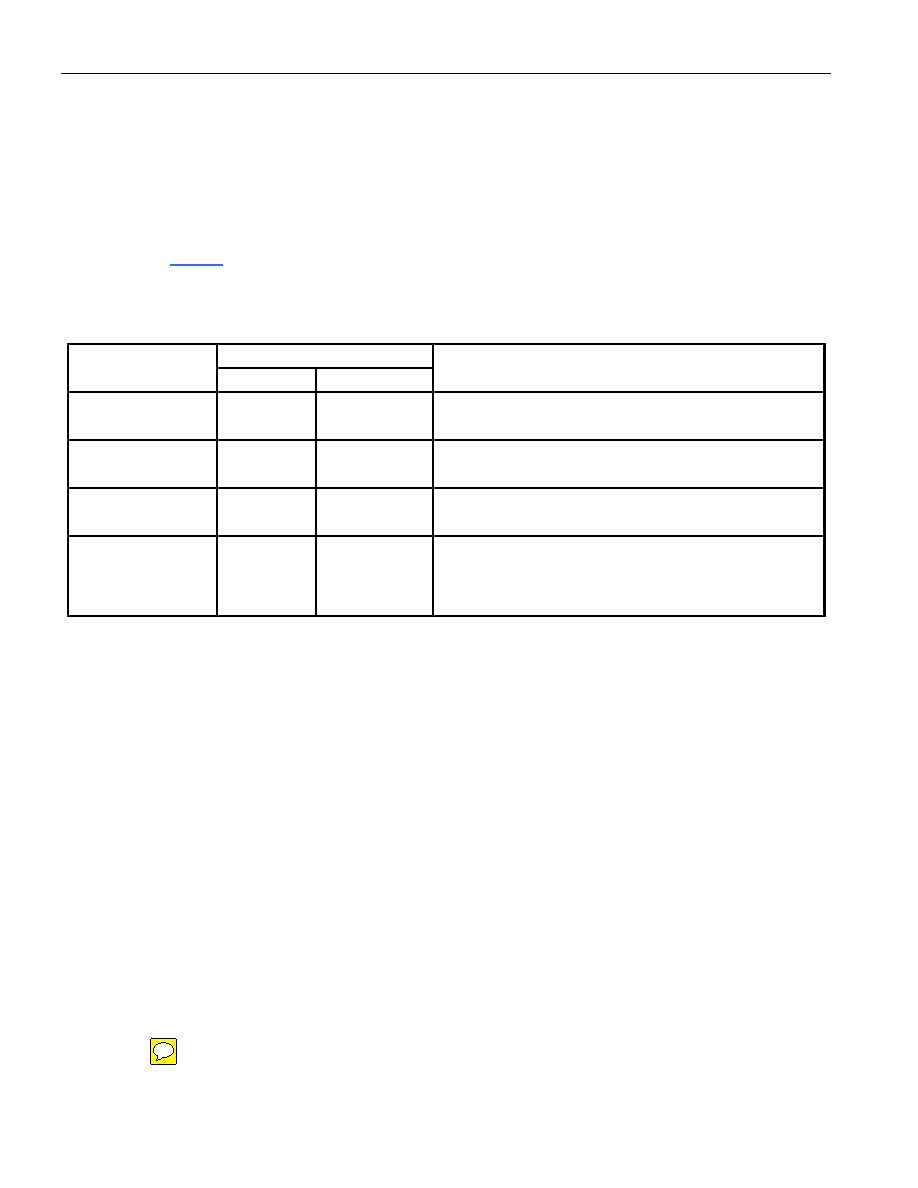
Table 6. Page Mode Select
CLOCKS PER MEMORY CYCLE
PAGES1:PAGES0
PAGE-HIT
PAGE-MISS
EXTERNAL BUS STRUCTURE
00
1
2
P0: Primary data bus.
P2: Primary address bus, multiplexing both the upper byte and
lower byte of address.
01
2
4
P0: Primary data bus.
P2: Primary address bus, multiplexing both the upper byte and
lower byte of address.
10
4
8
P0: Primary data bus.
P2: Primary address bus, multiplexing both the upper byte and
lower byte of address.
11
2
4
P0: Lower address byte.
P2: The upper address byte is multiplexed with the data byte.
Note: This setting affects external code fetches only; accessing
the external data memory requires four clock cycles, regardless
of page hit or miss.
The first page mode’s (page mode 1) external bus structure uses P2 as the primary address bus, (multiplexing both
the most significant byte and least significant byte of the address for each external memory cycle) and P0 is used
as the primary data bus. During external code fetches, P0 is held in a high-impedance state by the processor. Op
codes are driven by the external memory onto P0 and latched at the end of the external fetch cycle at the rising
edge of PSEN. During external data read/write operations, P0 functions as the data I/O bus. It is held in a high-
impedance state for external reads from data memory and driven with data during external writes to data memory.
A page miss occurs when the most significant byte of the subsequent address is different from the last
address. The external memory machine cycle can be 2, 4, or 8 system clocks in length for a page miss.
A page hit occurs when the most significant byte of the subsequent address does not change from the last
address. The external memory machine cycle can be 1, 2, or 4 system clocks in length for a page hit.
During a page hit, P2 drives Addr [0–7] of the 16-bit address, while the most significant address byte is held in the
external address latches. PSEN, RD, and WR strobes accordingly for the appropriate operation on the P0 data bus.
There is no ALE assertion for page hits.
相关PDF资料 |
PDF描述 |
|---|---|
| DS89C430-MNL | IC MCU FLASH 16KB 33MHZ 40-DIP |
| DS89C450-ENG+ | IC MCU FLASH 64KB 25MHZ 44-TQFP |
| DS89C450-MNG+ | IC MCU FLASH 64KB 25MHZ 40-DIP |
| VE-23R-CV | CONVERTER MOD DC/DC 7.5V 150W |
| DS89C450-MNG | IC MCU FLASH 64KB 25MHZ 40-DIP |
相关代理商/技术参数 |
参数描述 |
|---|---|
| DS89C430-MNL+ | 功能描述:8位微控制器 -MCU Ultra-High-Speed Flash MCU RoHS:否 制造商:Silicon Labs 核心:8051 处理器系列:C8051F39x 数据总线宽度:8 bit 最大时钟频率:50 MHz 程序存储器大小:16 KB 数据 RAM 大小:1 KB 片上 ADC:Yes 工作电源电压:1.8 V to 3.6 V 工作温度范围:- 40 C to + 105 C 封装 / 箱体:QFN-20 安装风格:SMD/SMT |
| DS89C430-QNG | 功能描述:8位微控制器 -MCU Ultra-High-Speed Flash MCU RoHS:否 制造商:Silicon Labs 核心:8051 处理器系列:C8051F39x 数据总线宽度:8 bit 最大时钟频率:50 MHz 程序存储器大小:16 KB 数据 RAM 大小:1 KB 片上 ADC:Yes 工作电源电压:1.8 V to 3.6 V 工作温度范围:- 40 C to + 105 C 封装 / 箱体:QFN-20 安装风格:SMD/SMT |
| DS89C430-QNG+ | 功能描述:8位微控制器 -MCU Ultra-High-Speed Flash MCU RoHS:否 制造商:Silicon Labs 核心:8051 处理器系列:C8051F39x 数据总线宽度:8 bit 最大时钟频率:50 MHz 程序存储器大小:16 KB 数据 RAM 大小:1 KB 片上 ADC:Yes 工作电源电压:1.8 V to 3.6 V 工作温度范围:- 40 C to + 105 C 封装 / 箱体:QFN-20 安装风格:SMD/SMT |
| DS89C430QNL | 制造商:Maxim Integrated Products 功能描述:Bulk |
| DS89C430-QNL | 功能描述:8位微控制器 -MCU Ultra-High-Speed Flash MCU RoHS:否 制造商:Silicon Labs 核心:8051 处理器系列:C8051F39x 数据总线宽度:8 bit 最大时钟频率:50 MHz 程序存储器大小:16 KB 数据 RAM 大小:1 KB 片上 ADC:Yes 工作电源电压:1.8 V to 3.6 V 工作温度范围:- 40 C to + 105 C 封装 / 箱体:QFN-20 安装风格:SMD/SMT |
发布紧急采购,3分钟左右您将得到回复。