参数资料
| 型号: | DSD1792DBRG4 |
| 厂商: | Texas Instruments |
| 文件页数: | 11/57页 |
| 文件大小: | 0K |
| 描述: | IC DAC 24BIT SER 28-SSOP |
| 产品培训模块: | Data Converter Basics |
| 标准包装: | 2,000 |
| 位数: | 24 |
| 数据接口: | 串行 |
| 转换器数目: | 2 |
| 电压电源: | 模拟和数字 |
| 功率耗散(最大): | 335mW |
| 工作温度: | -25°C ~ 85°C |
| 安装类型: | 表面贴装 |
| 封装/外壳: | 28-SSOP(0.209",5.30mm 宽) |
| 供应商设备封装: | 28-SSOP |
| 包装: | 带卷 (TR) |
| 输出数目和类型: | 4 电流,单极 |
| 采样率(每秒): | 200k |
第1页第2页第3页第4页第5页第6页第7页第8页第9页第10页当前第11页第12页第13页第14页第15页第16页第17页第18页第19页第20页第21页第22页第23页第24页第25页第26页第27页第28页第29页第30页第31页第32页第33页第34页第35页第36页第37页第38页第39页第40页第41页第42页第43页第44页第45页第46页第47页第48页第49页第50页第51页第52页第53页第54页第55页第56页第57页
DSD1792
SLES067B MARCH 2003 REVISED NOVEMBER 2006
www.ti.com
19
External Digital Filter Interface and Timing
The DSD1792 supports an external digital filter interface comprising a 3- or 4-wire synchronous serial port, which allows
the use of an external digital filter. External filters include the Texas Instruments’ DF1704 and DF1706, the Pacific
Microsonics PMD200, or a programmable digital signal processor.
In the external DF mode, PLRCK (pin 4), PBCK (pin 6) and PDATA (pin 5) are defined as WDCK, the word clock; BCK,
the bit clock; and DATA, the monaural data, respectively. The external digital filter interface is selected by using the DFTH
bit of control register 20, which functions to bypass the internal digital filter of the DSD1792.
When the DFMS bit of control register 19 is set, the DSD1792 can process stereo data. In this case, DSDL (pin 1) and DSDR
(pin 2) are defined as L-channel data and R-channel data, respectively.
Detailed information for the external digital filter interface mode is provided in the APPLICATION FOR EXTERNAL
DIGITAL FILTER INTERFACE section of this data sheet.
Direct Stream Digital (DSD) Format Interface and Timing
The DSD1792 supports the DSD-format interface operation, which includes out-of-band noise filtering using an internal
analog FIR filter. The DSD-format interface consists of a 3-wire synchronous serial port, which includes DBCK (pin 3),
DSDL (pin 1), and DSDR (pin 2). DBCK is the serial bit clock. DSDL and DSDR are L-channel and R-channel DSD data
input, respectively. They are clocked into the DSD1792 on the rising edge of DBCK. PLRCK (pin 4) and PBCK (pin 6) should
be connected to GND in the DSD mode. The DSD-(DSD mode) format interface is activated by setting the DSD bit of control
register 20.
Detailed information for the DSD mode is provided in the APPLICATION FOR DSD FORMAT (DSD MODE) INTERFACE
section of this data sheet.
TDMCA Interface
The DSD1792 supports the time-division-multiplexed command and audio (TDMCA) data format to enable control of and
communication with a number of external devices over a single serial interface.
Detailed information for the TDMCA format is provided in the TDMCA Format section of this data sheet.
Serial Control Interface
The serial control interface is a 4-wire synchronous serial port, which operates asynchronously with the serial audio
interface and the system clock (SCK). The serial control interface is used to program and read the on-chip mode registers.
The control interface includes MDO (pin 13), MDI (pin 11), MC (pin 12), and MS (pin 10). MDO is the serial data output,
used to read back the values of the mode registers; MDI is the serial data input, used to program the mode registers; MC
is the bit clock, used to shift data in and out of the control port, and MS is the mode control enable, used to enable the internal
mode register access.
Register Read/Write Operation
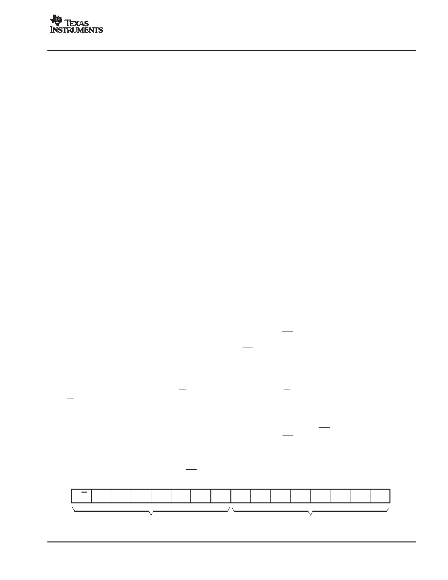
All read/write operations for the serial control port use 16-bit data words. Figure 29 shows the control data word format.
The most significant bit is the read/write (R/W) bit. For write operations, the R/W bit must be set to 0. For read operations,
the R/W bit must be set to 1. There are seven bits, labeled IDX[6:0], that set the register index (or address) for the read
and write operations. The least significant eight bits, D[7:0], contain the data to be written to the register specified by
IDX[6:0] or to be read from, the register specified by IDX[6:0].
Figure 30 shows the functional timing diagram for writing or reading the serial control port. MS is held at a logic 1 state until
a register needs to be written or read. To start the register write or read cycle, MS is set to logic 0. Sixteen clocks are then
provided on MC, corresponding to the 16 bits of the control data word on MDI and readback data on MDO. After the eighth
clock cycle has completed, the data from the indexed-mode control register appears on MDO during the read operation.
After the sixteenth clock cycle has completed, the data is latched into the indexed-mode control register during the write
operation. To write or read subsequent data, MS must be set to 1 once.
MSB
LSB
Register Index (or Address)
Register Data
R/W
IDX6
IDX5
IDX4
IDX3
IDX2
IDX1
IDX0
D7
D6
D4
D5
D3
D2
D1
D0
Figure 29. Control Data Word Format for MDI
相关PDF资料 |
PDF描述 |
|---|---|
| MS17345R20N29S | CONN PLUG 17POS FREE HNG W/SCKT |
| VI-2NT-IU-B1 | CONVERTER MOD DC/DC 6.5V 200W |
| DSD1792DBR | IC 24BIT STEREO AUD DAC 28-SSOP |
| VI-2NP-IU-B1 | CONVERTER MOD DC/DC 13.8V 200W |
| PCM1792DBRG4 | IC DAC 24BIT STER 192KHZ 28-SSOP |
相关代理商/技术参数 |
参数描述 |
|---|---|
| DSD1793 | 制造商:BB 制造商全称:BB 功能描述:24 BIT 192 KHZ SAMPLING ADVANCED SEGMENT AUDIO STEREO DIGITAL TO ANALOG CONVERTER |
| DSD1793DB | 功能描述:音频数/模转换器 IC 24-Bit 192kHz Smplng Adv Stg Stereo DAC RoHS:否 制造商:Texas Instruments 转换器数量: 分辨率:16 bit 接口类型:I2S, UBS 转换速率: 信噪比:98 dB 工作电源电压:5 V DAC 输出端数量:2 工作温度范围:- 25 C to + 85 C 电源电流:23 mA 安装风格:SMD/SMT 封装 / 箱体:TQFP-32 封装:Reel |
| DSD1793DBG4 | 功能描述:音频数/模转换器 IC 24B 192kHz Sampl Adv Segment Aud St DAC RoHS:否 制造商:Texas Instruments 转换器数量: 分辨率:16 bit 接口类型:I2S, UBS 转换速率: 信噪比:98 dB 工作电源电压:5 V DAC 输出端数量:2 工作温度范围:- 25 C to + 85 C 电源电流:23 mA 安装风格:SMD/SMT 封装 / 箱体:TQFP-32 封装:Reel |
| DSD1793DBR | 功能描述:音频数/模转换器 IC 24-Bit 192kHz Smplng Adv Stg Stereo DAC RoHS:否 制造商:Texas Instruments 转换器数量: 分辨率:16 bit 接口类型:I2S, UBS 转换速率: 信噪比:98 dB 工作电源电压:5 V DAC 输出端数量:2 工作温度范围:- 25 C to + 85 C 电源电流:23 mA 安装风格:SMD/SMT 封装 / 箱体:TQFP-32 封装:Reel |
| DSD1793DBRG4 | 功能描述:音频数/模转换器 IC 24-Bit 192kHz Smplng Adv Stg Stereo DAC RoHS:否 制造商:Texas Instruments 转换器数量: 分辨率:16 bit 接口类型:I2S, UBS 转换速率: 信噪比:98 dB 工作电源电压:5 V DAC 输出端数量:2 工作温度范围:- 25 C to + 85 C 电源电流:23 mA 安装风格:SMD/SMT 封装 / 箱体:TQFP-32 封装:Reel |
发布紧急采购,3分钟左右您将得到回复。