- 您现在的位置:买卖IC网 > PDF目录19356 > DSP56321VF240 (Freescale Semiconductor)IC DSP 24BIT 240MHZ 196-BGA PDF资料下载
参数资料
| 型号: | DSP56321VF240 |
| 厂商: | Freescale Semiconductor |
| 文件页数: | 26/84页 |
| 文件大小: | 0K |
| 描述: | IC DSP 24BIT 240MHZ 196-BGA |
| 标准包装: | 126 |
| 系列: | DSP56K/Symphony |
| 类型: | 定点 |
| 接口: | 主机接口,SSI,SCI |
| 时钟速率: | 240MHz |
| 非易失内存: | ROM(576 B) |
| 芯片上RAM: | 576kB |
| 电压 - 输入/输出: | 3.30V |
| 电压 - 核心: | 1.60V |
| 工作温度: | -40°C ~ 100°C |
| 安装类型: | 表面贴装 |
| 封装/外壳: | 196-FBGA |
| 供应商设备封装: | 196-MAPBGA(15x15) |
| 包装: | 托盘 |
第1页第2页第3页第4页第5页第6页第7页第8页第9页第10页第11页第12页第13页第14页第15页第16页第17页第18页第19页第20页第21页第22页第23页第24页第25页当前第26页第27页第28页第29页第30页第31页第32页第33页第34页第35页第36页第37页第38页第39页第40页第41页第42页第43页第44页第45页第46页第47页第48页第49页第50页第51页第52页第53页第54页第55页第56页第57页第58页第59页第60页第61页第62页第63页第64页第65页第66页第67页第68页第69页第70页第71页第72页第73页第74页第75页第76页第77页第78页第79页第80页第81页第82页第83页第84页
DSP56321 Technical Data, Rev. 11
2-12
Freescale Semiconductor
Specifications
115 Address valid to RD
assertion
—0.5
× TC 2.0
0.5
—
0.3
—
0.1
—
–0.18
—
ns
116 RD assertion pulse width
—
(WS + 0.25)
× TC 3.0
[WS
≥ 3]
13.25
—
11.59
—
10.55
—
8.81
—
ns
117 RD deassertion to
address not valid
—1.25
× TC 4.0
[3
≤WS ≤7]
2.25
× T
C 4.0
[WS
≥ 8]
2.25
7.25
—
1.69
6.24
—
1.21
5.38
—
0.54
4.18
—
ns
118 TA setup before RD or
WR deassertion5
—0.25
× T
C + 2.0
3.25
—
3.14
—
3.04
—
2.91
—
ns
119 TA hold after RD or WR
deassertion
—
0
—0
—
0
—
ns
Notes:
1.
WS is the number of wait states specified in the BCR. The value is given for the minimum for a given category. (For example,
for a category of [3
≤WS ≤7] timing is specified for 3 wait states.) Three wait states is the minimum value otherwise.
2.
Timings 100 and 107 are guaranteed by design, not tested.
3.
All timings are measured from 0.5
× V
CCQH to 0.5 × VCCQH.
4.
The WS number applies to the access in which the deassertion of WR occurs and assumes the next access uses a minimal
number of wait states.
5.
Timing 118 is relative to the deassertion edge of RD or WR even if TA remains asserted.
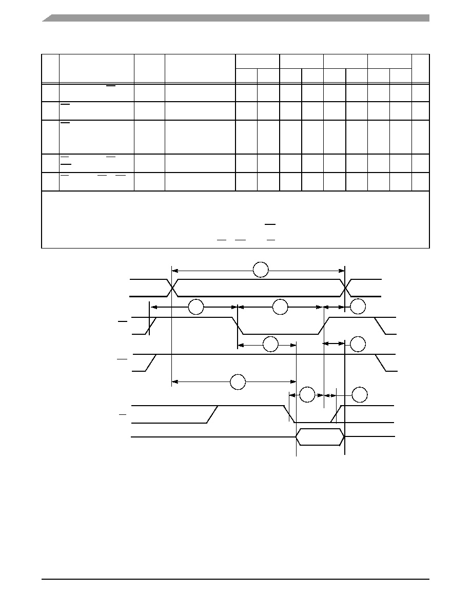
Figure 2-10.
SRAM Read Access
Table 2-8.
SRAM Timing (Continued)
No.
Characteristics
Symbol
Expression1
200 MHz
220 MHz
240 MHz
275 MHz
Unit
Min
Max
Min
Max
Min
Max
Min
Max
A[0–17]
RD
WR
D[0–23]
AA[0–3]
105
106
113
104
116
117
100
TA
118
Data
In
119
Note: Address lines A[0–17] hold their state after a
read or write operation. AA[0–3] do not hold their
state after a read or write operation.
相关PDF资料 |
PDF描述 |
|---|---|
| ATFC-0402-1N8-BT | INDUCTOR THIN FILM 1.8NH 0402 |
| VJ1206Y221KBBAT4X | CAP CER 220PF 100V 10% X7R 1206 |
| GBA06DTMD | CONN EDGECARD 12POS R/A .125 SLD |
| VE-BTL-CV-F2 | CONVERTER MOD DC/DC 28V 150W |
| JWS240P24/508 | PWR SUP 24V 10A SNG OUTPUT |
相关代理商/技术参数 |
参数描述 |
|---|---|
| DSP56321VF275 | 功能描述:数字信号处理器和控制器 - DSP, DSC 275Mhz/550MMACS 275Mhz EFCOP RoHS:否 制造商:Microchip Technology 核心:dsPIC 数据总线宽度:16 bit 程序存储器大小:16 KB 数据 RAM 大小:2 KB 最大时钟频率:40 MHz 可编程输入/输出端数量:35 定时器数量:3 设备每秒兆指令数:50 MIPs 工作电源电压:3.3 V 最大工作温度:+ 85 C 封装 / 箱体:TQFP-44 安装风格:SMD/SMT |
| DSP56321VL200 | 功能描述:数字信号处理器和控制器 - DSP, DSC 24 BIT DSP PBFREE RoHS:否 制造商:Microchip Technology 核心:dsPIC 数据总线宽度:16 bit 程序存储器大小:16 KB 数据 RAM 大小:2 KB 最大时钟频率:40 MHz 可编程输入/输出端数量:35 定时器数量:3 设备每秒兆指令数:50 MIPs 工作电源电压:3.3 V 最大工作温度:+ 85 C 封装 / 箱体:TQFP-44 安装风格:SMD/SMT |
| DSP56321VL200R2 | 功能描述:数字信号处理器和控制器 - DSP, DSC 24 BIT DSP PBFREE RoHS:否 制造商:Microchip Technology 核心:dsPIC 数据总线宽度:16 bit 程序存储器大小:16 KB 数据 RAM 大小:2 KB 最大时钟频率:40 MHz 可编程输入/输出端数量:35 定时器数量:3 设备每秒兆指令数:50 MIPs 工作电源电压:3.3 V 最大工作温度:+ 85 C 封装 / 箱体:TQFP-44 安装风格:SMD/SMT |
| DSP56321VL220 | 功能描述:数字信号处理器和控制器 - DSP, DSC 24 BIT DSP PBFREE RoHS:否 制造商:Microchip Technology 核心:dsPIC 数据总线宽度:16 bit 程序存储器大小:16 KB 数据 RAM 大小:2 KB 最大时钟频率:40 MHz 可编程输入/输出端数量:35 定时器数量:3 设备每秒兆指令数:50 MIPs 工作电源电压:3.3 V 最大工作温度:+ 85 C 封装 / 箱体:TQFP-44 安装风格:SMD/SMT |
| DSP56321VL240 | 功能描述:数字信号处理器和控制器 - DSP, DSC 24 BIT DSP PBFREE RoHS:否 制造商:Microchip Technology 核心:dsPIC 数据总线宽度:16 bit 程序存储器大小:16 KB 数据 RAM 大小:2 KB 最大时钟频率:40 MHz 可编程输入/输出端数量:35 定时器数量:3 设备每秒兆指令数:50 MIPs 工作电源电压:3.3 V 最大工作温度:+ 85 C 封装 / 箱体:TQFP-44 安装风格:SMD/SMT |
发布紧急采购,3分钟左右您将得到回复。