- 您现在的位置:买卖IC网 > PDF目录19361 > DSP56321VL200 (Freescale Semiconductor)IC DSP 24BIT 200MHZ 196-MAPBGA PDF资料下载
参数资料
| 型号: | DSP56321VL200 |
| 厂商: | Freescale Semiconductor |
| 文件页数: | 39/84页 |
| 文件大小: | 0K |
| 描述: | IC DSP 24BIT 200MHZ 196-MAPBGA |
| 标准包装: | 126 |
| 系列: | DSP56K/Symphony |
| 类型: | 定点 |
| 接口: | 主机接口,SSI,SCI |
| 时钟速率: | 200MHz |
| 非易失内存: | ROM(576 B) |
| 芯片上RAM: | 576kB |
| 电压 - 输入/输出: | 3.30V |
| 电压 - 核心: | 1.60V |
| 工作温度: | -40°C ~ 100°C |
| 安装类型: | 表面贴装 |
| 封装/外壳: | 196-FBGA |
| 供应商设备封装: | 196-MAPBGA(15x15) |
| 包装: | 托盘 |
第1页第2页第3页第4页第5页第6页第7页第8页第9页第10页第11页第12页第13页第14页第15页第16页第17页第18页第19页第20页第21页第22页第23页第24页第25页第26页第27页第28页第29页第30页第31页第32页第33页第34页第35页第36页第37页第38页当前第39页第40页第41页第42页第43页第44页第45页第46页第47页第48页第49页第50页第51页第52页第53页第54页第55页第56页第57页第58页第59页第60页第61页第62页第63页第64页第65页第66页第67页第68页第69页第70页第71页第72页第73页第74页第75页第76页第77页第78页第79页第80页第81页第82页第83页第84页
DSP56321 Technical Data, Rev. 11
2-24
Freescale Semiconductor
Specifications
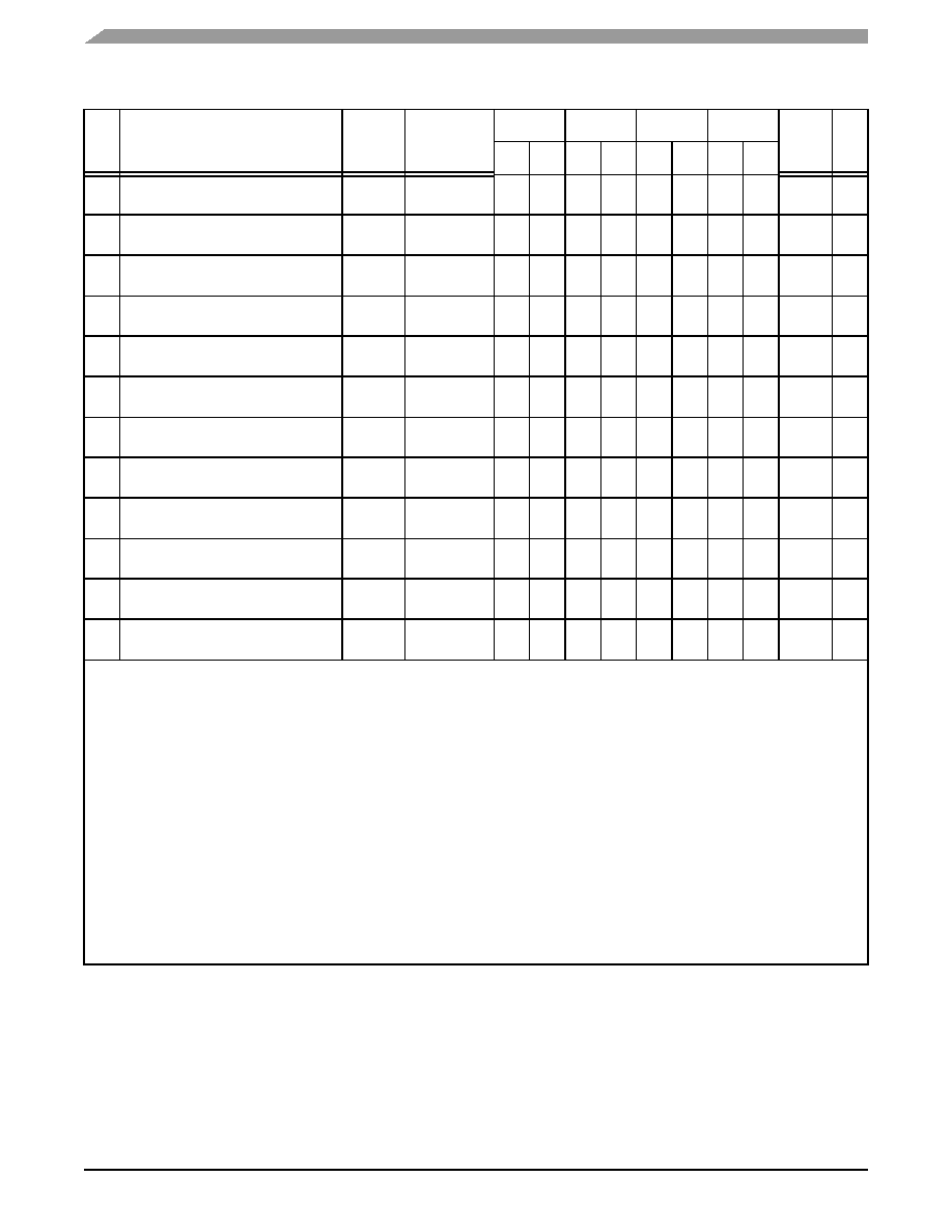
451 TXC rising edge to FST out (word-
length) low
—
12.5
8.3
—
12.5
8.3
—
12.5
8.3
—
12.5
8.3
x ck
i ck
ns
452 TXC rising edge to data out enable from
high impedance
—
12.5
8.3
—
12.5
8.3
—
12.5
8.3
—
12.5
8.3
x ck
i ck
ns
453 TXC rising edge to Transmitter 0 drive
enable assertion
—
12.5
13.5
—
12.5
13.5
—
12.5
13.5
—
12.5
13.5
x ck
i ck
ns
454 TXC rising edge to data out valid
—
12.5
8.3
—
12.5
8.3
—
12.5
8.3
—
12.5
8.3
x ck
i ck
ns
455 TXC rising edge to data out high
impedance
3
—
30.0
8.3
—
30.0
8.3
—
30.0
8.3
—
30.0
8.3
x ck
i ck
ns
456 TXC rising edge to Transmitter 0 drive
enable deassertion3
—
12.5
8.3
—
12.5
8.3
—
12.5
8.3
—
12.5
8.3
x ck
i ck
ns
457 FST input (bl, wr) setup time before
TXC falling edge2
5.0
10.0
—
5.0
10.0
—
5.0
10.0
—
5.0
10.0
—
x ck
i ck
ns
458 FST input (wl) to data out enable from
high impedance
—
15.0
8.0
—
15.0
8.0
—
15.0
8.0
—
15.0
8.0
x ck
i ck
ns
459 FST input (wl) to Transmitter 0 drive
enable assertion
—
15.0
18.0
—
15.0
18.0
—
15.0
18.0
—
15.0
18.0
x ck
i ck
ns
460 FST input (wl) setup time before TXC
falling edge
5.0
10.0
—
5.0
10.0
—
5.0
10.0
—
5.0
10.0
—
x ck
i ck
ns
461 FST input hold time after TXC falling
edge
3.8
5.0
—
3.8
5.0
—
3.8
5.0
—
3.8
5.0
—
x ck
i ck
ns
462 Flag output valid after TXC rising edge
—
12.5
8.3
—
12.5
8.3
—
12.5
8.3
—
12.5
8.3
x ck
i ck
ns
Notes:
1.
For the internal clock, the external clock cycle is defined by the instruction cycle time (timing 7 in Table 2-5 on page 2-4) and the
ESSI control register. TECCX must be ≥ TC × 3, in accordance with the note below Table 7-1 in the DSP56321 Reference
Manual. TECCI must be ≥ TC × 4, in accordance with the explanation of CRA[PSR] and the ESSI Clock Generator Functional
Block Diagram shown in Figure 7-3 of the DSP56321 Reference Manual.
2.
The word-length-relative frame sync signal waveform operates the same way as the bit-length frame sync signal waveform, but
spreads from one serial clock before the first bit clock (same as the Bit Length Frame Sync signal) until the one before last bit
clock of the first word in the frame.
3.
Periodically sampled and not 100 percent tested
4.
VCCQH = 3.3 V ± 0.3 V, VCCQL = 1.6 V ± 0.1 V; TJ = 0°C to +85°C, CL = 50 pF
5.
TXC (SCK Pin) = Transmit Clock
RXC (SC0 or SCK Pin) = Receive Clock
FST (SC2 Pin) = Transmit Frame Sync
FSR (SC1 or SC2 Pin) Receive Frame Sync
6.
i ck = Internal Clock; x ck = External Clock
i ck a = Internal Clock, Asynchronous Mode (asynchronous implies that TXC and RXC are two different clocks)
i ck s = Internal Clock, Synchronous Mode (synchronous implies that TXC and RXC are the same clock)
7.
In the timing diagrams below, the clocks and frame sync signals are drawn using the clock falling edge as a the first reference.
Clock and frame sync polarities are programmable in Control Register B (CRB). Refer to the
DSP56321 Reference Manual for
details.
Table 2-12.
ESSI Timings (Continued)
No.
Characteristics4, 6
Symbol Expression
200 MHz
220 MHz
240 MHz
275 MHz
Cond-
ition5
Unit
Min Max Min Max Min Max Min Max
相关PDF资料 |
PDF描述 |
|---|---|
| AGM30DRSN-S288 | CONN EDGECARD EXTEND 60POS .156 |
| IRS2168DPBF | IC PFC BALLAST CTLR ADV 16-PDIP |
| EP4CE6F17I8LN | IC CYCLONE IV E FPGA 6K 256FBGA |
| T525D227M004ATE025 | CAP TANT 220UF 4V 20% 2917 |
| TPSD686M016R0150 | CAP TANT 68UF 16V 20% 2917 |
相关代理商/技术参数 |
参数描述 |
|---|---|
| DSP56321VL200R2 | 功能描述:数字信号处理器和控制器 - DSP, DSC 24 BIT DSP PBFREE RoHS:否 制造商:Microchip Technology 核心:dsPIC 数据总线宽度:16 bit 程序存储器大小:16 KB 数据 RAM 大小:2 KB 最大时钟频率:40 MHz 可编程输入/输出端数量:35 定时器数量:3 设备每秒兆指令数:50 MIPs 工作电源电压:3.3 V 最大工作温度:+ 85 C 封装 / 箱体:TQFP-44 安装风格:SMD/SMT |
| DSP56321VL220 | 功能描述:数字信号处理器和控制器 - DSP, DSC 24 BIT DSP PBFREE RoHS:否 制造商:Microchip Technology 核心:dsPIC 数据总线宽度:16 bit 程序存储器大小:16 KB 数据 RAM 大小:2 KB 最大时钟频率:40 MHz 可编程输入/输出端数量:35 定时器数量:3 设备每秒兆指令数:50 MIPs 工作电源电压:3.3 V 最大工作温度:+ 85 C 封装 / 箱体:TQFP-44 安装风格:SMD/SMT |
| DSP56321VL240 | 功能描述:数字信号处理器和控制器 - DSP, DSC 24 BIT DSP PBFREE RoHS:否 制造商:Microchip Technology 核心:dsPIC 数据总线宽度:16 bit 程序存储器大小:16 KB 数据 RAM 大小:2 KB 最大时钟频率:40 MHz 可编程输入/输出端数量:35 定时器数量:3 设备每秒兆指令数:50 MIPs 工作电源电压:3.3 V 最大工作温度:+ 85 C 封装 / 箱体:TQFP-44 安装风格:SMD/SMT |
| DSP56321VL275 | 功能描述:数字信号处理器和控制器 - DSP, DSC 24 BIT DSP PBFREE RoHS:否 制造商:Microchip Technology 核心:dsPIC 数据总线宽度:16 bit 程序存储器大小:16 KB 数据 RAM 大小:2 KB 最大时钟频率:40 MHz 可编程输入/输出端数量:35 定时器数量:3 设备每秒兆指令数:50 MIPs 工作电源电压:3.3 V 最大工作温度:+ 85 C 封装 / 箱体:TQFP-44 安装风格:SMD/SMT |
| DSP56321VL275 | 制造商:Freescale Semiconductor 功能描述:Digital Signal Processor (DSP) IC |
发布紧急采购,3分钟左右您将得到回复。