- 您现在的位置:买卖IC网 > PDF目录19294 > DSP56321VL200R2 (Freescale Semiconductor)IC DSP 24BIT 200MHZ 196-MAPBGA PDF资料下载
参数资料
| 型号: | DSP56321VL200R2 |
| 厂商: | Freescale Semiconductor |
| 文件页数: | 14/84页 |
| 文件大小: | 0K |
| 描述: | IC DSP 24BIT 200MHZ 196-MAPBGA |
| 标准包装: | 750 |
| 系列: | DSP56K/Symphony |
| 类型: | 定点 |
| 接口: | 主机接口,SSI,SCI |
| 时钟速率: | 200MHz |
| 非易失内存: | ROM(576 B) |
| 芯片上RAM: | 576kB |
| 电压 - 输入/输出: | 3.30V |
| 电压 - 核心: | 1.60V |
| 工作温度: | -40°C ~ 100°C |
| 安装类型: | 表面贴装 |
| 封装/外壳: | 196-FBGA |
| 供应商设备封装: | 196-MAPBGA(15x15) |
| 包装: | 带卷 (TR) |
第1页第2页第3页第4页第5页第6页第7页第8页第9页第10页第11页第12页第13页当前第14页第15页第16页第17页第18页第19页第20页第21页第22页第23页第24页第25页第26页第27页第28页第29页第30页第31页第32页第33页第34页第35页第36页第37页第38页第39页第40页第41页第42页第43页第44页第45页第46页第47页第48页第49页第50页第51页第52页第53页第54页第55页第56页第57页第58页第59页第60页第61页第62页第63页第64页第65页第66页第67页第68页第69页第70页第71页第72页第73页第74页第75页第76页第77页第78页第79页第80页第81页第82页第83页第84页
DSP56321 Technical Data, Rev. 11
Freescale Semiconductor
2-1
Specifications
2
The DSP56321 is fabricated in high-density CMOS with Transistor-Transistor Logic (TTL) compatible inputs and
outputs.
2.1 Maximum Ratings
In the calculation of timing requirements, adding a maximum value of one specification to a minimum value of
another specification does not yield a reasonable sum. A maximum specification is calculated using a worst case
variation of process parameter values in one direction. The minimum specification is calculated using the worst
case for the same parameters in the opposite direction. Therefore, a “maximum” value for a specification never
occurs in the same device that has a “minimum” value for another specification; adding a maximum to a minimum
represents a condition that can never exist.
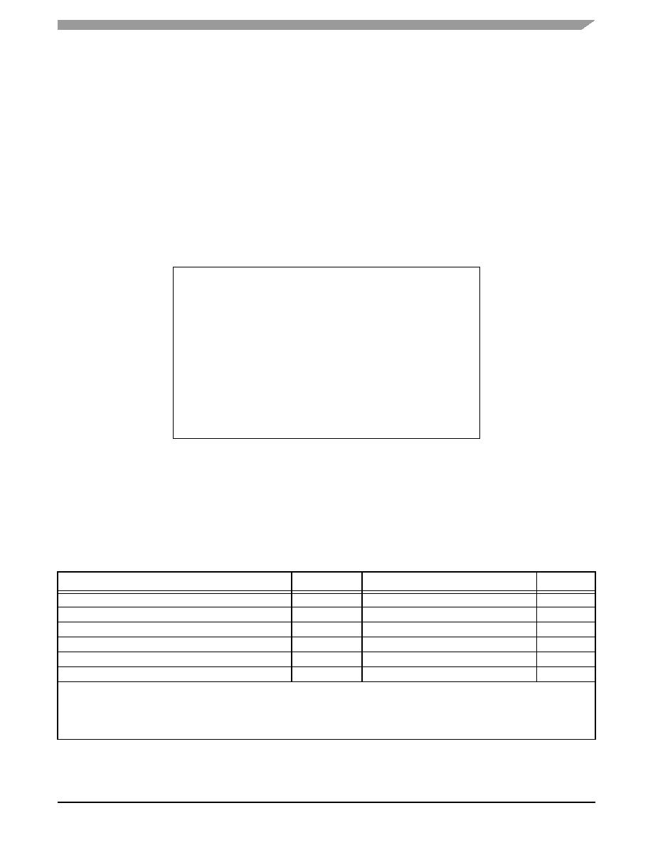
CAUTION
This
device
contains
circuitry
protecting
against damage due to high static voltage or
electrical fields; however, normal precautions
should be taken to avoid exceeding maximum
voltage ratings. Reliability is enhanced if
unused inputs are tied to an appropriate logic
voltage level (for example, either GND or VCC).
Table 2-1.
Absolute Maximum Ratings
Rating1
Symbol
Value1, 2
Unit
Supply Voltage3
VCCQL
–0.1 to 2.25
V
Input/Output Supply Voltage
3
VCCQH
–0.3 to 4.35
V
All input voltages
VIN
GND – 0.3 to VCCQH + 0.3
V
Current drain per pin excluding VCC and GND
I
10
mA
Operating temperature range
TJ
–40 to +100
°C
Storage temperature
TSTG
–55 to +150
°C
Notes:
1.
GND = 0 V, VCCQL = 1.6 V ± 0.1 V, VCCQH = 3.3 V ± 0.3 V, TJ = –40°C to +100°C, CL = 50 pF
2.
Absolute maximum ratings are stress ratings only, and functional operation at the maximum is not guaranteed. Stress beyond
the maximum rating may affect device reliability or cause permanent damage to the device.
3.
Power-up sequence: During power-up, and throughout the DSP56321 operation, VCCQH voltage must always be higher or
equal to VCCQL voltage.
相关PDF资料 |
PDF描述 |
|---|---|
| HSC49DREH | CONN EDGECARD 98POS .100 EYELET |
| TACA336M010RTA | CAP TANT 33UF 10V 20% 1206 |
| ECC23DJXN-S1136 | CONN EDGECARD 46PS .100 PRESSFIT |
| VJ1206A271KBBAT4X | CAP CER 270PF 100V 10% NP0 1206 |
| GEC15DREN | CONN EDGECARD 30POS .100 EYELET |
相关代理商/技术参数 |
参数描述 |
|---|---|
| DSP56321VL220 | 功能描述:数字信号处理器和控制器 - DSP, DSC 24 BIT DSP PBFREE RoHS:否 制造商:Microchip Technology 核心:dsPIC 数据总线宽度:16 bit 程序存储器大小:16 KB 数据 RAM 大小:2 KB 最大时钟频率:40 MHz 可编程输入/输出端数量:35 定时器数量:3 设备每秒兆指令数:50 MIPs 工作电源电压:3.3 V 最大工作温度:+ 85 C 封装 / 箱体:TQFP-44 安装风格:SMD/SMT |
| DSP56321VL240 | 功能描述:数字信号处理器和控制器 - DSP, DSC 24 BIT DSP PBFREE RoHS:否 制造商:Microchip Technology 核心:dsPIC 数据总线宽度:16 bit 程序存储器大小:16 KB 数据 RAM 大小:2 KB 最大时钟频率:40 MHz 可编程输入/输出端数量:35 定时器数量:3 设备每秒兆指令数:50 MIPs 工作电源电压:3.3 V 最大工作温度:+ 85 C 封装 / 箱体:TQFP-44 安装风格:SMD/SMT |
| DSP56321VL275 | 功能描述:数字信号处理器和控制器 - DSP, DSC 24 BIT DSP PBFREE RoHS:否 制造商:Microchip Technology 核心:dsPIC 数据总线宽度:16 bit 程序存储器大小:16 KB 数据 RAM 大小:2 KB 最大时钟频率:40 MHz 可编程输入/输出端数量:35 定时器数量:3 设备每秒兆指令数:50 MIPs 工作电源电压:3.3 V 最大工作温度:+ 85 C 封装 / 箱体:TQFP-44 安装风格:SMD/SMT |
| DSP56321VL275 | 制造商:Freescale Semiconductor 功能描述:Digital Signal Processor (DSP) IC |
| DSP56362 | 制造商:FREESCALE 制造商全称:Freescale Semiconductor, Inc 功能描述:24-Bit Audio Digital Signal Processor |
发布紧急采购,3分钟左右您将得到回复。