- 您现在的位置:买卖IC网 > PDF目录11427 > DSPIC30F3010T-30I/SO (Microchip Technology)IC DSPIC MCU/DSP 24K 28SOIC PDF资料下载
参数资料
| 型号: | DSPIC30F3010T-30I/SO |
| 厂商: | Microchip Technology |
| 文件页数: | 49/66页 |
| 文件大小: | 0K |
| 描述: | IC DSPIC MCU/DSP 24K 28SOIC |
| 产品培训模块: | Asynchronous Stimulus |
| 标准包装: | 1,600 |
| 系列: | dsPIC™ 30F |
| 核心处理器: | dsPIC |
| 芯体尺寸: | 16-位 |
| 速度: | 30 MIP |
| 连通性: | I²C,SPI,UART/USART |
| 外围设备: | 高级欠压探测/复位,电机控制 PWM,QEI,POR,PWM,WDT |
| 输入/输出数: | 20 |
| 程序存储器容量: | 24KB(8K x 24) |
| 程序存储器类型: | 闪存 |
| EEPROM 大小: | 1K x 8 |
| RAM 容量: | 1K x 8 |
| 电压 - 电源 (Vcc/Vdd): | 2.5 V ~ 5.5 V |
| 数据转换器: | A/D 6x10b |
| 振荡器型: | 内部 |
| 工作温度: | -40°C ~ 85°C |
| 封装/外壳: | 28-SOIC(0.295",7.50mm 宽) |
| 包装: | 带卷 (TR) |
第1页第2页第3页第4页第5页第6页第7页第8页第9页第10页第11页第12页第13页第14页第15页第16页第17页第18页第19页第20页第21页第22页第23页第24页第25页第26页第27页第28页第29页第30页第31页第32页第33页第34页第35页第36页第37页第38页第39页第40页第41页第42页第43页第44页第45页第46页第47页第48页当前第49页第50页第51页第52页第53页第54页第55页第56页第57页第58页第59页第60页第61页第62页第63页第64页第65页第66页
2010 Microchip Technology Inc.
DS70102K-page 53
dsPIC30F Flash Programming Specification
11.13 Reading the Application ID Word
The application ID word is stored at address 0x8005BE
in executive code memory. To read this memory
location, you must use the SIX control code to move
this program memory location to the VISI register. The
REGOUT control code must then be used to clock the
contents of the VISI register out of the device. The
corresponding control and instruction codes that must
be serially transmitted to the device to perform this
operation are shown in Table 11-13.
Once the programmer has clocked-out the application
ID word, it must be inspected. If the application ID has
the value 0xBB, the programming executive is resident
in memory and the device can be programmed using
the mechanism described in Section 5.0 “Device
Programming”. However, if the application ID has any
other value, the programming executive is not resident
in memory. It must be loaded to memory before the
device can be programmed. The procedure for loading
the programming executive to the memory is described
11.14 Exiting ICSP Mode
After confirming that the programming executive is
resident in memory, or loading the programming
executive, ICSP mode is exited by removing power to
the device or bringing MCLR to VIL. Programming can
then take place by following the procedure outlined in
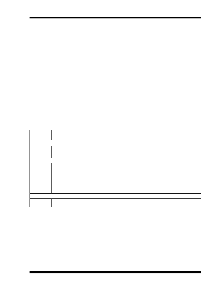
TABLE 11-13: SERIAL INSTRUCTION EXECUTION FOR READING THE APPLICATION ID WORD
Command
(Binary)
Data
(Hexadecimal)
Description
Step 1: Exit the Reset vector.
0000
040100
000000
GOTO 0x100
NOP
Step 2: Initialize TBLPAG and the read pointer (W0) for TBLRD instruction.
0000
200800
880190
205BE0
207841
000000
BA0890
000000
MOV
#0x80, W0
MOV
W0, TBLPAG
MOV
#0x5BE, W0
MOV
VISI, W1
NOP
TBLRDL [W0], [W1]
NOP
Step 3: Output the VISI register using the REGOUT command.
0001
0000
<VISI>
000000
Clock out contents of the VISI register
NOP
相关PDF资料 |
PDF描述 |
|---|---|
| PIC18F66K22-E/MR | IC MCU PIC 64K FLASH XLP 64QFN |
| PIC18F65K80-E/MR | MCU PIC 32KB FLASH ECAN 64QFN |
| DSPIC33FJ16GS404-E/PT | IC DSPIC MCU/DSP 16K 44-TQFP |
| PIC24FJ96GA010-I/PT | IC PIC MCU FLASH 96KB 100TQFP |
| PIC16C55-10/P | IC MCU OTP 512X12 28DIP |
相关代理商/技术参数 |
参数描述 |
|---|---|
| dsPIC30F3011-20E/ML | 功能描述:数字信号处理器和控制器 - DSP, DSC 44LD 20MIPS 24 KB RoHS:否 制造商:Microchip Technology 核心:dsPIC 数据总线宽度:16 bit 程序存储器大小:16 KB 数据 RAM 大小:2 KB 最大时钟频率:40 MHz 可编程输入/输出端数量:35 定时器数量:3 设备每秒兆指令数:50 MIPs 工作电源电压:3.3 V 最大工作温度:+ 85 C 封装 / 箱体:TQFP-44 安装风格:SMD/SMT |
| dsPIC30F3011-20E/P | 功能描述:数字信号处理器和控制器 - DSP, DSC 40LD 20MIPS 24 KB RoHS:否 制造商:Microchip Technology 核心:dsPIC 数据总线宽度:16 bit 程序存储器大小:16 KB 数据 RAM 大小:2 KB 最大时钟频率:40 MHz 可编程输入/输出端数量:35 定时器数量:3 设备每秒兆指令数:50 MIPs 工作电源电压:3.3 V 最大工作温度:+ 85 C 封装 / 箱体:TQFP-44 安装风格:SMD/SMT |
| dsPIC30F3011-20E/PT | 功能描述:数字信号处理器和控制器 - DSP, DSC 20MIPS 24 KB RoHS:否 制造商:Microchip Technology 核心:dsPIC 数据总线宽度:16 bit 程序存储器大小:16 KB 数据 RAM 大小:2 KB 最大时钟频率:40 MHz 可编程输入/输出端数量:35 定时器数量:3 设备每秒兆指令数:50 MIPs 工作电源电压:3.3 V 最大工作温度:+ 85 C 封装 / 箱体:TQFP-44 安装风格:SMD/SMT |
| dsPIC30F3011-20I/ML | 功能描述:数字信号处理器和控制器 - DSP, DSC 44LD 20MIPS 24 KB RoHS:否 制造商:Microchip Technology 核心:dsPIC 数据总线宽度:16 bit 程序存储器大小:16 KB 数据 RAM 大小:2 KB 最大时钟频率:40 MHz 可编程输入/输出端数量:35 定时器数量:3 设备每秒兆指令数:50 MIPs 工作电源电压:3.3 V 最大工作温度:+ 85 C 封装 / 箱体:TQFP-44 安装风格:SMD/SMT |
| dsPIC30F3011-20I/P | 功能描述:数字信号处理器和控制器 - DSP, DSC 40LD 20MIPS 24 KB RoHS:否 制造商:Microchip Technology 核心:dsPIC 数据总线宽度:16 bit 程序存储器大小:16 KB 数据 RAM 大小:2 KB 最大时钟频率:40 MHz 可编程输入/输出端数量:35 定时器数量:3 设备每秒兆指令数:50 MIPs 工作电源电压:3.3 V 最大工作温度:+ 85 C 封装 / 箱体:TQFP-44 安装风格:SMD/SMT |
发布紧急采购,3分钟左右您将得到回复。