- 您现在的位置:买卖IC网 > PDF目录11727 > DSPIC30F6013-30I/PF (Microchip Technology)IC DSPIC MCU/DSP 132K 80TQFP PDF资料下载
参数资料
| 型号: | DSPIC30F6013-30I/PF |
| 厂商: | Microchip Technology |
| 文件页数: | 63/228页 |
| 文件大小: | 0K |
| 描述: | IC DSPIC MCU/DSP 132K 80TQFP |
| 产品培训模块: | Serial Communications using dsPIC30F CAN Serial Communications using dsPIC30F I2C Serial Communications using dsPIC30F SPI Serial Communications using dsPIC30F UART dsPIC30F 12 bit ADC - Part 2 dsPIC30F Addressing Modes - Part 1 dsPIC30F Architecture - Part 1 dsPIC30F DSP Engine & ALU dsPIC30F Interrupts dsPIC30F Motor Control PWM dsPIC Timers Asynchronous Stimulus dsPIC30F Addressing Modes - Part 2 dsPIC30F Architecture - Part 2 dsPIC30F 12-bit ADC Part 1 |
| 标准包装: | 90 |
| 系列: | dsPIC™ 30F |
| 核心处理器: | dsPIC |
| 芯体尺寸: | 16-位 |
| 速度: | 30 MIP |
| 连通性: | CAN,I²C,SPI,UART/USART |
| 外围设备: | 欠压检测/复位,LVD,POR,PWM,WDT |
| 输入/输出数: | 68 |
| 程序存储器容量: | 132KB(44K x 24) |
| 程序存储器类型: | 闪存 |
| EEPROM 大小: | 2K x 8 |
| RAM 容量: | 6K x 8 |
| 电压 - 电源 (Vcc/Vdd): | 2.5 V ~ 5.5 V |
| 数据转换器: | A/D 16x12b |
| 振荡器型: | 内部 |
| 工作温度: | -40°C ~ 85°C |
| 封装/外壳: | 80-TQFP |
| 包装: | 托盘 |
| 产品目录页面: | 651 (CN2011-ZH PDF) |
| 配用: | DM300024-ND - KIT DEMO DSPICDEM 1.1 AC164314-ND - MODULE SKT FOR PM3 80PF DV164005-ND - KIT ICD2 SIMPLE SUIT W/USB CABLE |
| 其它名称: | DSPIC30F601330IPF |
第1页第2页第3页第4页第5页第6页第7页第8页第9页第10页第11页第12页第13页第14页第15页第16页第17页第18页第19页第20页第21页第22页第23页第24页第25页第26页第27页第28页第29页第30页第31页第32页第33页第34页第35页第36页第37页第38页第39页第40页第41页第42页第43页第44页第45页第46页第47页第48页第49页第50页第51页第52页第53页第54页第55页第56页第57页第58页第59页第60页第61页第62页当前第63页第64页第65页第66页第67页第68页第69页第70页第71页第72页第73页第74页第75页第76页第77页第78页第79页第80页第81页第82页第83页第84页第85页第86页第87页第88页第89页第90页第91页第92页第93页第94页第95页第96页第97页第98页第99页第100页第101页第102页第103页第104页第105页第106页第107页第108页第109页第110页第111页第112页第113页第114页第115页第116页第117页第118页第119页第120页第121页第122页第123页第124页第125页第126页第127页第128页第129页第130页第131页第132页第133页第134页第135页第136页第137页第138页第139页第140页第141页第142页第143页第144页第145页第146页第147页第148页第149页第150页第151页第152页第153页第154页第155页第156页第157页第158页第159页第160页第161页第162页第163页第164页第165页第166页第167页第168页第169页第170页第171页第172页第173页第174页第175页第176页第177页第178页第179页第180页第181页第182页第183页第184页第185页第186页第187页第188页第189页第190页第191页第192页第193页第194页第195页第196页第197页第198页第199页第200页第201页第202页第203页第204页第205页第206页第207页第208页第209页第210页第211页第212页第213页第214页第215页第216页第217页第218页第219页第220页第221页第222页第223页第224页第225页第226页第227页第228页
2006 Microchip Technology Inc.
DS70117F-page 153
dsPIC30F6011/6012/6013/6014
20.3.1.1
POR with Long Crystal Start-up Time
(with FSCM Enabled)
The oscillator start-up circuitry is not linked to the POR
circuitry. Some crystal circuits (especially low fre-
quency crystals) will have a relatively long start-up
time. Therefore, one or more of the following conditions
is possible after the POR timer and the PWRT have
expired:
The oscillator circuit has not begun to oscillate.
The Oscillator Start-up Timer has not expired (if a
crystal oscillator is used).
The PLL has not achieved a LOCK (if PLL is
used).
If the FSCM is enabled and one of the above conditions
is true, then a clock failure trap will occur. The device
will automatically switch to the FRC oscillator and the
user can switch to the desired crystal oscillator in the
trap ISR.
20.3.1.2
Operating without FSCM and PWRT
If the FSCM is disabled and the Power-up Timer
(PWRT) is also disabled, then the device will exit rap-
idly from Reset on power-up. If the clock source is
FRC, LPRC, EXTRC or EC, it will be active
immediately.
If the FSCM is disabled and the system clock has not
started, the device will be in a frozen state at the Reset
vector until the system clock starts. From the user’s
perspective, the device will appear to be in Reset until
a system clock is available.
20.3.2
BOR: PROGRAMMABLE
BROWN-OUT RESET
The BOR (Brown-out Reset) module is based on an
internal voltage reference circuit. The main purpose of
the BOR module is to generate a device Reset when a
brown-out condition occurs. Brown-out conditions are
generally caused by glitches on the AC mains (i.e.,
missing portions of the AC cycle waveform due to bad
power transmission lines, or voltage sags due to exces-
sive current draw when a large inductive load is turned
on).
The BOR module allows selection of one of the
following voltage trip points (see Table 23-11):
2.6V-2.71V
4.1V-4.4V
4.58V-4.73V
A BOR will generate a Reset pulse which will reset the
device. The BOR will select the clock source based on
the device Configuration bit values (FOS<1:0> and
FPR<3:0>). Furthermore, if an Oscillator mode is
selected, the BOR will activate the Oscillator Start-up
Timer (OST). The system clock is held until OST
expires. If the PLL is used, then the clock will be held
until the LOCK bit (OSCCON<5>) is ‘1’.
Concurrently, the POR time-out (TPOR) and the PWRT
time-out (TPWRT) will be applied before the internal Reset
is released. If TPWRT = 0 and a crystal oscillator is being
used, then a nominal delay of TFSCM = 100
μs is applied.
The total delay in this case is (TPOR + TFSCM).
The BOR status bit (RCON<1>) will be set to indicate
that a BOR has occurred. The BOR circuit, if enabled,
will continue to operate while in Sleep or Idle modes
and will reset the device should VDD fall below the BOR
threshold voltage.
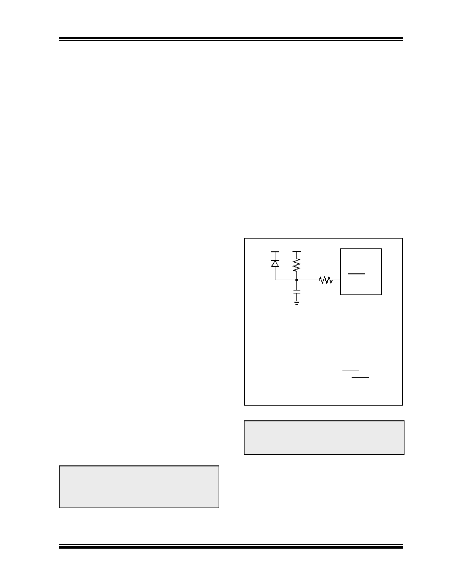
FIGURE 20-6:
EXTERNAL POWER-ON
RESET CIRCUIT (FOR
SLOW VDD POWER-UP)
Note:
The BOR voltage trip points indicated here
are nominal values provided for design
guidance only. Refer to the Electrical
Specifications in the specific device data
sheet for BOR voltage limit specifications.
Note:
Dedicated supervisory devices, such as
the MCP1XX and MCP8XX, may also be
used as an external Power-on Reset
circuit.
Note
1:
External Power-on Reset circuit is required
only if the VDD power-up slope is too slow.
The diode D helps discharge the capacitor
quickly when VDD powers down.
2:
R should be suitably chosen so as to make
sure that the voltage drop across R does not
violate the device’s electrical specifications.
3:
R1 should be suitably chosen so as to limit
any current flowing into MCLR from external
capacitor C, in the event of MCLR/VPP pin
breakdown due to Electrostatic Discharge
(ESD), or Electrical Overstress (EOS).
C
R1
R
D
VDD
dsPIC30F
MCLR
相关PDF资料 |
PDF描述 |
|---|---|
| 31-212-RFX | BNC PLUG CLAMP, RG-59 |
| V24C12M100B3 | CONVERTER MOD DC/DC 12V 100W |
| GJM1555C1H8R0CB01D | CAP CER 8PF 50V NP0 0402 |
| VE-B4N-IX-F1 | CONVERTER MOD DC/DC 18.5V 75W |
| V375C12H150BG3 | CONVERTER MOD DC/DC 12V 150W |
相关代理商/技术参数 |
参数描述 |
|---|---|
| dsPIC30F6013A-20E/PF | 功能描述:数字信号处理器和控制器 - DSP, DSC 20MIPS 132 KB RoHS:否 制造商:Microchip Technology 核心:dsPIC 数据总线宽度:16 bit 程序存储器大小:16 KB 数据 RAM 大小:2 KB 最大时钟频率:40 MHz 可编程输入/输出端数量:35 定时器数量:3 设备每秒兆指令数:50 MIPs 工作电源电压:3.3 V 最大工作温度:+ 85 C 封装 / 箱体:TQFP-44 安装风格:SMD/SMT |
| dsPIC30F6013A-20E/PT | 功能描述:数字信号处理器和控制器 - DSP, DSC 20MIPS 132 KB RoHS:否 制造商:Microchip Technology 核心:dsPIC 数据总线宽度:16 bit 程序存储器大小:16 KB 数据 RAM 大小:2 KB 最大时钟频率:40 MHz 可编程输入/输出端数量:35 定时器数量:3 设备每秒兆指令数:50 MIPs 工作电源电压:3.3 V 最大工作温度:+ 85 C 封装 / 箱体:TQFP-44 安装风格:SMD/SMT |
| DSPIC30F6013A-20I/PT | 功能描述:IC DSPIC MCU/DSP 132K 80TQFP RoHS:否 类别:集成电路 (IC) >> 嵌入式 - 微控制器, 系列:dsPIC™ 30F 产品培训模块:XLP Deep Sleep Mode 8-bit PIC® Microcontroller Portfolio 标准包装:22 系列:PIC® XLP™ 18F 核心处理器:PIC 芯体尺寸:8-位 速度:48MHz 连通性:I²C,SPI,UART/USART,USB 外围设备:欠压检测/复位,POR,PWM,WDT 输入/输出数:14 程序存储器容量:8KB(4K x 16) 程序存储器类型:闪存 EEPROM 大小:256 x 8 RAM 容量:512 x 8 电压 - 电源 (Vcc/Vdd):1.8 V ~ 5.5 V 数据转换器:A/D 11x10b 振荡器型:内部 工作温度:-40°C ~ 85°C 封装/外壳:20-DIP(0.300",7.62mm) 包装:管件 产品目录页面:642 (CN2011-ZH PDF) 配用:DV164126-ND - KIT DEVELOPMENT USB W/PICKIT 2DM164127-ND - KIT DEVELOPMENT USB 18F14/13K50AC164112-ND - VOLTAGE LIMITER MPLAB ICD2 VPP |
| DSPIC30F6013A-20I/PTG | 制造商:Microchip Technology Inc 功能描述:16BIT 20MIPS DSPIC SMD 30F6013 |
| dsPIC30F6013A-30I/PF | 功能描述:数字信号处理器和控制器 - DSP, DSC 30MIPS 132 KB RoHS:否 制造商:Microchip Technology 核心:dsPIC 数据总线宽度:16 bit 程序存储器大小:16 KB 数据 RAM 大小:2 KB 最大时钟频率:40 MHz 可编程输入/输出端数量:35 定时器数量:3 设备每秒兆指令数:50 MIPs 工作电源电压:3.3 V 最大工作温度:+ 85 C 封装 / 箱体:TQFP-44 安装风格:SMD/SMT |
发布紧急采购,3分钟左右您将得到回复。