- 您现在的位置:买卖IC网 > PDF目录11453 > DSPIC33FJ12MC202-E/ML (Microchip Technology)IC DSPIC MCU/DSP 12K 28QFN PDF资料下载
参数资料
| 型号: | DSPIC33FJ12MC202-E/ML |
| 厂商: | Microchip Technology |
| 文件页数: | 144/155页 |
| 文件大小: | 0K |
| 描述: | IC DSPIC MCU/DSP 12K 28QFN |
| 产品培训模块: | Asynchronous Stimulus |
| 标准包装: | 61 |
| 系列: | dsPIC™ 33F |
| 核心处理器: | dsPIC |
| 芯体尺寸: | 16-位 |
| 速度: | 40 MIP |
| 连通性: | I²C,IrDA,SPI,UART/USART |
| 外围设备: | 高级欠压探测/复位,电机控制 PWM,QEI,POR,PWM,WDT |
| 输入/输出数: | 21 |
| 程序存储器容量: | 12KB(12K x 8) |
| 程序存储器类型: | 闪存 |
| RAM 容量: | 1K x 8 |
| 电压 - 电源 (Vcc/Vdd): | 3 V ~ 3.6 V |
| 数据转换器: | A/D 6x10b/12b |
| 振荡器型: | 内部 |
| 工作温度: | -40°C ~ 125°C |
| 封装/外壳: | 28-VQFN 裸露焊盘 |
| 包装: | 管件 |
| 配用: | AC164336-ND - MODULE SOCKET FOR PM3 28/44QFN DM240001-ND - BOARD DEMO PIC24/DSPIC33/PIC32 |
第1页第2页第3页第4页第5页第6页第7页第8页第9页第10页第11页第12页第13页第14页第15页第16页第17页第18页第19页第20页第21页第22页第23页第24页第25页第26页第27页第28页第29页第30页第31页第32页第33页第34页第35页第36页第37页第38页第39页第40页第41页第42页第43页第44页第45页第46页第47页第48页第49页第50页第51页第52页第53页第54页第55页第56页第57页第58页第59页第60页第61页第62页第63页第64页第65页第66页第67页第68页第69页第70页第71页第72页第73页第74页第75页第76页第77页第78页第79页第80页第81页第82页第83页第84页第85页第86页第87页第88页第89页第90页第91页第92页第93页第94页第95页第96页第97页第98页第99页第100页第101页第102页第103页第104页第105页第106页第107页第108页第109页第110页第111页第112页第113页第114页第115页第116页第117页第118页第119页第120页第121页第122页第123页第124页第125页第126页第127页第128页第129页第130页第131页第132页第133页第134页第135页第136页第137页第138页第139页第140页第141页第142页第143页当前第144页第145页第146页第147页第148页第149页第150页第151页第152页第153页第154页第155页
89
A/T89C51AC2
4127H–8051–02/08
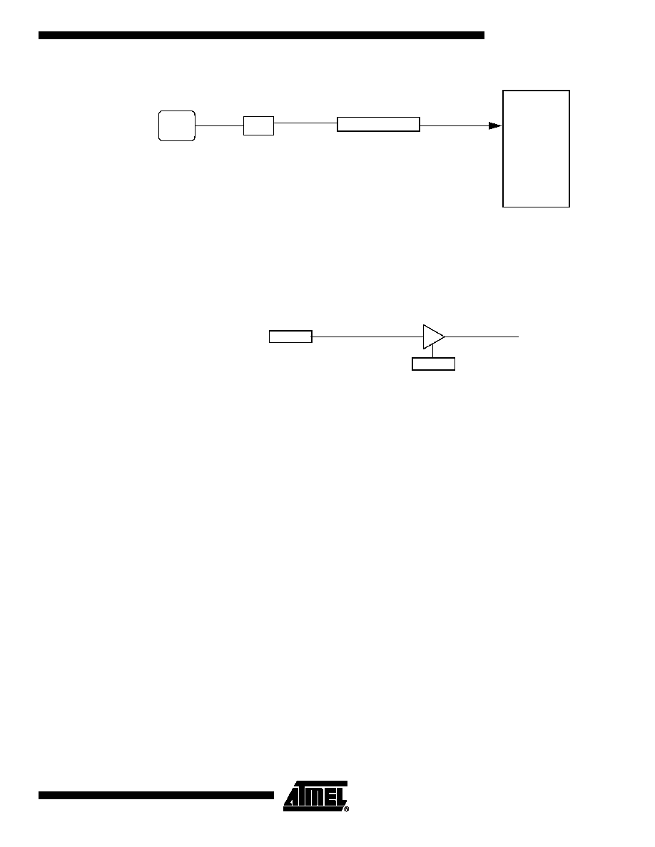
Figure 47. A/D Converter clock
ADC Standby Mode
When the ADC is not used, it is possible to set it in standby mode by clearing bit ADEN
in ADCON register. In this mode its power dissipation is reduced.
IT ADC Management
An interrupt end-of-conversion will occurs when the bit ADEOC is activated and the bit
EADC is set. For re-arming the interrupt the bit ADEOC must be cleared by software.
Figure 48. ADC Interrupt Structure
Routines examples
1.
Configure P1.2 and P1.3 in ADC channels
// configure channel P1.2 and P1.3 for ADC
ADCF = 0Ch
// Enable the ADC
ADCON = 20h
2.
Start a standard conversion
// The variable "channel" contains the channel to convert
// The variable "value_converted" is an unsigned int
// Clear the field SCH[2:0]
ADCON and = F8h
// Select channel
ADCON | = channel
// Start conversion in standard mode
ADCON | = 08h
// Wait flag End of conversion
while((ADCON and 01h)! = 01h)
// Clear the End of conversion flag
ADCON and = EFh
// read the value
value_converted = (ADDH << 2)+(ADDL)
3.
Start a precision conversion (need interrupt ADC)
// The variable "channel" contains the channel to convert
// Enable ADC
EADC = 1
Prescaler ADCLK
A/D
Converter
ADC Clock
CPU
CLOCK
CPU Core Clock Symbol
÷ 2
ADEOC
ADCON.2
EADC
IEN1.1
ADCI
相关PDF资料 |
PDF描述 |
|---|---|
| DSPIC30F2012-20E/ML | IC DSPIC MCU/DSP 12K 28QFN |
| PIC24FJ64GA102T-I/SS | MCU 64KB FLASH 8KB RAM 28SSOP |
| PIC24EP64MC203T-E/TL | IC MCU 16BIT 64KB FLASH 36-VTLA |
| DSPIC33EP64MC203T-E/TL | IC DSC 16BIT 64KB FLASH 36-VTLA |
| PIC32MX230F064B-V/SS | IC MCU 32BIT 64KB FLASH 28SSOP |
相关代理商/技术参数 |
参数描述 |
|---|---|
| dsPIC33FJ12MC202-I/ML | 功能描述:数字信号处理器和控制器 - DSP, DSC 212KB Flash 1024BRAM 40MIPS RoHS:否 制造商:Microchip Technology 核心:dsPIC 数据总线宽度:16 bit 程序存储器大小:16 KB 数据 RAM 大小:2 KB 最大时钟频率:40 MHz 可编程输入/输出端数量:35 定时器数量:3 设备每秒兆指令数:50 MIPs 工作电源电压:3.3 V 最大工作温度:+ 85 C 封装 / 箱体:TQFP-44 安装风格:SMD/SMT |
| dsPIC33FJ12MC202-I/SO | 功能描述:数字信号处理器和控制器 - DSP, DSC 212KB Flash 1024BRAM 40MIPS RoHS:否 制造商:Microchip Technology 核心:dsPIC 数据总线宽度:16 bit 程序存储器大小:16 KB 数据 RAM 大小:2 KB 最大时钟频率:40 MHz 可编程输入/输出端数量:35 定时器数量:3 设备每秒兆指令数:50 MIPs 工作电源电压:3.3 V 最大工作温度:+ 85 C 封装 / 箱体:TQFP-44 安装风格:SMD/SMT |
| dsPIC33FJ12MC202-I/SP | 功能描述:数字信号处理器和控制器 - DSP, DSC 12KB Flash 1024byte RAM 16B RoHS:否 制造商:Microchip Technology 核心:dsPIC 数据总线宽度:16 bit 程序存储器大小:16 KB 数据 RAM 大小:2 KB 最大时钟频率:40 MHz 可编程输入/输出端数量:35 定时器数量:3 设备每秒兆指令数:50 MIPs 工作电源电压:3.3 V 最大工作温度:+ 85 C 封装 / 箱体:TQFP-44 安装风格:SMD/SMT |
| dsPIC33FJ12MC202-I/SS | 功能描述:数字信号处理器和控制器 - DSP, DSC 12kb Flash 1024BYTES 40MIPS 21 I/O RoHS:否 制造商:Microchip Technology 核心:dsPIC 数据总线宽度:16 bit 程序存储器大小:16 KB 数据 RAM 大小:2 KB 最大时钟频率:40 MHz 可编程输入/输出端数量:35 定时器数量:3 设备每秒兆指令数:50 MIPs 工作电源电压:3.3 V 最大工作温度:+ 85 C 封装 / 箱体:TQFP-44 安装风格:SMD/SMT |
| dsPIC33FJ12MC202T-E/ML | 功能描述:数字信号处理器和控制器 - DSP, DSC 12KB FLSH 1024BRAM 16B nanoWatt RoHS:否 制造商:Microchip Technology 核心:dsPIC 数据总线宽度:16 bit 程序存储器大小:16 KB 数据 RAM 大小:2 KB 最大时钟频率:40 MHz 可编程输入/输出端数量:35 定时器数量:3 设备每秒兆指令数:50 MIPs 工作电源电压:3.3 V 最大工作温度:+ 85 C 封装 / 箱体:TQFP-44 安装风格:SMD/SMT |
发布紧急采购,3分钟左右您将得到回复。