- 您现在的位置:买卖IC网 > PDF目录21170 > DSPIC33FJ256GP510T-I/PF (Microchip Technology)IC DSPIC MCU/DSP 256K 100TQFP PDF资料下载
参数资料
| 型号: | DSPIC33FJ256GP510T-I/PF |
| 厂商: | Microchip Technology |
| 文件页数: | 169/197页 |
| 文件大小: | 0K |
| 描述: | IC DSPIC MCU/DSP 256K 100TQFP |
| 产品培训模块: | Asynchronous Stimulus |
| 标准包装: | 1,000 |
| 系列: | dsPIC™ 33F |
| 核心处理器: | dsPIC |
| 芯体尺寸: | 16-位 |
| 速度: | 40 MIP |
| 连通性: | CAN,I²C,IrDA,LIN,SPI,UART/USART |
| 外围设备: | AC'97,欠压检测/复位,DMA,I²S,POR,PWM,WDT |
| 输入/输出数: | 85 |
| 程序存储器容量: | 256KB(256K x 8) |
| 程序存储器类型: | 闪存 |
| RAM 容量: | 16K x 8 |
| 电压 - 电源 (Vcc/Vdd): | 3 V ~ 3.6 V |
| 数据转换器: | A/D 32x10b/12b |
| 振荡器型: | 内部 |
| 工作温度: | -40°C ~ 85°C |
| 封装/外壳: | 100-TQFP |
| 包装: | 带卷 (TR) |
| 配用: | DM300024-ND - KIT DEMO DSPICDEM 1.1 DV164033-ND - KIT START EXPLORER 16 MPLAB ICD2 MA330012-ND - MODULE DSPIC33 100P TO 84QFP MA330011-ND - MODULE DSPIC33 100P TO 100QFP DM240001-ND - BOARD DEMO PIC24/DSPIC33/PIC32 AC164323-ND - MODULE SKT FOR 100TQFP |
第1页第2页第3页第4页第5页第6页第7页第8页第9页第10页第11页第12页第13页第14页第15页第16页第17页第18页第19页第20页第21页第22页第23页第24页第25页第26页第27页第28页第29页第30页第31页第32页第33页第34页第35页第36页第37页第38页第39页第40页第41页第42页第43页第44页第45页第46页第47页第48页第49页第50页第51页第52页第53页第54页第55页第56页第57页第58页第59页第60页第61页第62页第63页第64页第65页第66页第67页第68页第69页第70页第71页第72页第73页第74页第75页第76页第77页第78页第79页第80页第81页第82页第83页第84页第85页第86页第87页第88页第89页第90页第91页第92页第93页第94页第95页第96页第97页第98页第99页第100页第101页第102页第103页第104页第105页第106页第107页第108页第109页第110页第111页第112页第113页第114页第115页第116页第117页第118页第119页第120页第121页第122页第123页第124页第125页第126页第127页第128页第129页第130页第131页第132页第133页第134页第135页第136页第137页第138页第139页第140页第141页第142页第143页第144页第145页第146页第147页第148页第149页第150页第151页第152页第153页第154页第155页第156页第157页第158页第159页第160页第161页第162页第163页第164页第165页第166页第167页第168页当前第169页第170页第171页第172页第173页第174页第175页第176页第177页第178页第179页第180页第181页第182页第183页第184页第185页第186页第187页第188页第189页第190页第191页第192页第193页第194页第195页第196页第197页
2009 Microchip Technology Inc.
DS70286C-page 71
dsPIC33FJXXXGPX06/X08/X10
5.0
FLASH PROGRAM MEMORY
The dsPIC33FJXXXGPX06/X08/X10 devices contain
internal Flash program memory for storing and
executing application code. The memory is readable,
writable and erasable during normal operation over the
entire VDD range.
Flash memory can be programmed in two ways:
1.
In-Circuit Serial Programming (ICSP)
programming capability
2.
Run-Time Self-Programming (RTSP)
ICSP allows a dsPIC33FJXXXGPX06/X08/X10 device
to be serially programmed while in the end application
circuit. This is simply done with two lines for
programming clock and programming data (one of the
alternate programming pin pairs: PGECx/PGEDx), and
three other lines for power (VDD), ground (VSS) and
Master Clear (MCLR). This allows customers to manu-
facture boards with unprogrammed devices and then
program the digital signal controller just before shipping
the product. This also allows the most recent firmware
or a custom firmware to be programmed.
RTSP is accomplished using TBLRD (table read) and
TBLWT
(table write) instructions. With RTSP, the user
can write program memory data either in blocks or
‘rows’ of 64 instructions (192 bytes) at a time or a single
program memory word, and erase program memory in
blocks or ‘pages’ of 512 instructions (1536 bytes) at a
time.
5.1
Table Instructions and Flash
Programming
Regardless of the method used, all programming of
Flash memory is done with the table read and table
write instructions. These allow direct read and write
access to the program memory space from the data
memory while the device is in normal operating mode.
The 24-bit target address in the program memory is
formed using bits<7:0> of the TBLPAG register and the
Effective Address (EA) from a W register specified in
the table instruction, as shown in Figure 5-1.
The TBLRDL and the TBLWTL instructions are used to
read or write to bits<15:0> of program memory.
TBLRDL
and TBLWTL can access program memory in
both Word and Byte modes.
The TBLRDH and TBLWTH instructions are used to read
or write to bits<23:16> of program memory. TBLRDH
and TBLWTH can also access program memory in Word
or Byte mode.
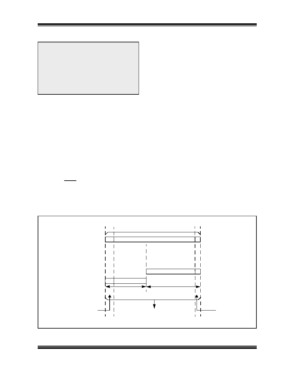
FIGURE 5-1:
ADDRESSING FOR TABLE REGISTERS
Note:
This data sheet summarizes the features
of the dsPIC33FJXXXGPX06/X08/X10
family of devices. However, it is not
intended to be a comprehensive reference
source. To complement the information in
this data sheet, refer to Section 5. “Flash
Programming”
(DS70191)
in
the
“dsPIC33F Family Reference Manual”,
which is available from the Microchip web
site (www.microchip.com).
0
Program Counter
24 bits
Program Counter
TBLPAG Reg
8 bits
Working Reg EA
16 bits
Byte
24-bit EA
0
1/0
Select
Using
Table Instruction
Using
User/Configuration
Space Select
相关PDF资料 |
PDF描述 |
|---|---|
| P51-2000-S-S-MD-20MA-000-000 | SENSOR 2000PSIS 1/4 NPT 4-20 MA |
| P51-1500-A-A-M12-4.5V-000-000 | SENSOR 1500PSI 1/4-18NPT .5-4.5V |
| P51-200-S-W-I12-20MA-000-000 | SENSOR 200PSIS 1/8 NPT 4-20 MA |
| P51-300-G-U-I12-4.5V-000-000 | SENSOR 300PSI 7/16-20-2B .5-4.5V |
| P51-1000-A-A-M12-4.5V-000-000 | SENSOR 1000PSI 1/4-18NPT .5-4.5V |
相关代理商/技术参数 |
参数描述 |
|---|---|
| dsPIC33FJ256GP710A-E/PF | 功能描述:数字信号处理器和控制器 - DSP, DSC 16Bit 40MIPS 256KB Flash RoHS:否 制造商:Microchip Technology 核心:dsPIC 数据总线宽度:16 bit 程序存储器大小:16 KB 数据 RAM 大小:2 KB 最大时钟频率:40 MHz 可编程输入/输出端数量:35 定时器数量:3 设备每秒兆指令数:50 MIPs 工作电源电压:3.3 V 最大工作温度:+ 85 C 封装 / 箱体:TQFP-44 安装风格:SMD/SMT |
| dsPIC33FJ256GP710A-E/PT | 功能描述:数字信号处理器和控制器 - DSP, DSC 16Bit 40MIPS 256KB Flash RoHS:否 制造商:Microchip Technology 核心:dsPIC 数据总线宽度:16 bit 程序存储器大小:16 KB 数据 RAM 大小:2 KB 最大时钟频率:40 MHz 可编程输入/输出端数量:35 定时器数量:3 设备每秒兆指令数:50 MIPs 工作电源电压:3.3 V 最大工作温度:+ 85 C 封装 / 箱体:TQFP-44 安装风格:SMD/SMT |
| dsPIC33FJ256GP710A-H/PF | 功能描述:数字信号处理器和控制器 - DSP, DSC 16 bit DSC 20MIPS 256KB Flash RoHS:否 制造商:Microchip Technology 核心:dsPIC 数据总线宽度:16 bit 程序存储器大小:16 KB 数据 RAM 大小:2 KB 最大时钟频率:40 MHz 可编程输入/输出端数量:35 定时器数量:3 设备每秒兆指令数:50 MIPs 工作电源电压:3.3 V 最大工作温度:+ 85 C 封装 / 箱体:TQFP-44 安装风格:SMD/SMT |
| dsPIC33FJ256GP710A-H/PT | 功能描述:数字信号处理器和控制器 - DSP, DSC 16 bit DSC 20MIPS 256KB Flash RoHS:否 制造商:Microchip Technology 核心:dsPIC 数据总线宽度:16 bit 程序存储器大小:16 KB 数据 RAM 大小:2 KB 最大时钟频率:40 MHz 可编程输入/输出端数量:35 定时器数量:3 设备每秒兆指令数:50 MIPs 工作电源电压:3.3 V 最大工作温度:+ 85 C 封装 / 箱体:TQFP-44 安装风格:SMD/SMT |
| dsPIC33FJ256GP710A-I/PF | 功能描述:数字信号处理器和控制器 - DSP, DSC 16Bit 40MIPS 256KB Flash RoHS:否 制造商:Microchip Technology 核心:dsPIC 数据总线宽度:16 bit 程序存储器大小:16 KB 数据 RAM 大小:2 KB 最大时钟频率:40 MHz 可编程输入/输出端数量:35 定时器数量:3 设备每秒兆指令数:50 MIPs 工作电源电压:3.3 V 最大工作温度:+ 85 C 封装 / 箱体:TQFP-44 安装风格:SMD/SMT |
发布紧急采购,3分钟左右您将得到回复。