- 您现在的位置:买卖IC网 > PDF目录21281 > DSPIC33FJ256MC510T-I/PT (Microchip Technology)IC DSPIC MCU/DSP 256K 100TQFP PDF资料下载
参数资料
| 型号: | DSPIC33FJ256MC510T-I/PT |
| 厂商: | Microchip Technology |
| 文件页数: | 100/136页 |
| 文件大小: | 0K |
| 描述: | IC DSPIC MCU/DSP 256K 100TQFP |
| 产品培训模块: | Asynchronous Stimulus |
| 标准包装: | 1,200 |
| 系列: | dsPIC™ 33F |
| 核心处理器: | dsPIC |
| 芯体尺寸: | 16-位 |
| 速度: | 40 MIP |
| 连通性: | CAN,I²C,IrDA,LIN,SPI,UART/USART |
| 外围设备: | 欠压检测/复位,DMA,电机控制 PWM,QEI,POR,PWM,WDT |
| 输入/输出数: | 85 |
| 程序存储器容量: | 256KB(256K x 8) |
| 程序存储器类型: | 闪存 |
| RAM 容量: | 16K x 8 |
| 电压 - 电源 (Vcc/Vdd): | 3 V ~ 3.6 V |
| 数据转换器: | A/D 24x10b/12b |
| 振荡器型: | 内部 |
| 工作温度: | -40°C ~ 85°C |
| 封装/外壳: | 100-TQFP |
| 包装: | 带卷 (TR) |
| 配用: | MA330013-ND - MODULE PLUG-IN DSPIC33 100TQFP DV164033-ND - KIT START EXPLORER 16 MPLAB ICD2 DM240001-ND - BOARD DEMO PIC24/DSPIC33/PIC32 |
第1页第2页第3页第4页第5页第6页第7页第8页第9页第10页第11页第12页第13页第14页第15页第16页第17页第18页第19页第20页第21页第22页第23页第24页第25页第26页第27页第28页第29页第30页第31页第32页第33页第34页第35页第36页第37页第38页第39页第40页第41页第42页第43页第44页第45页第46页第47页第48页第49页第50页第51页第52页第53页第54页第55页第56页第57页第58页第59页第60页第61页第62页第63页第64页第65页第66页第67页第68页第69页第70页第71页第72页第73页第74页第75页第76页第77页第78页第79页第80页第81页第82页第83页第84页第85页第86页第87页第88页第89页第90页第91页第92页第93页第94页第95页第96页第97页第98页第99页当前第100页第101页第102页第103页第104页第105页第106页第107页第108页第109页第110页第111页第112页第113页第114页第115页第116页第117页第118页第119页第120页第121页第122页第123页第124页第125页第126页第127页第128页第129页第130页第131页第132页第133页第134页第135页第136页
66
4235K–8051–05/08
AT89C51RD2/ED2
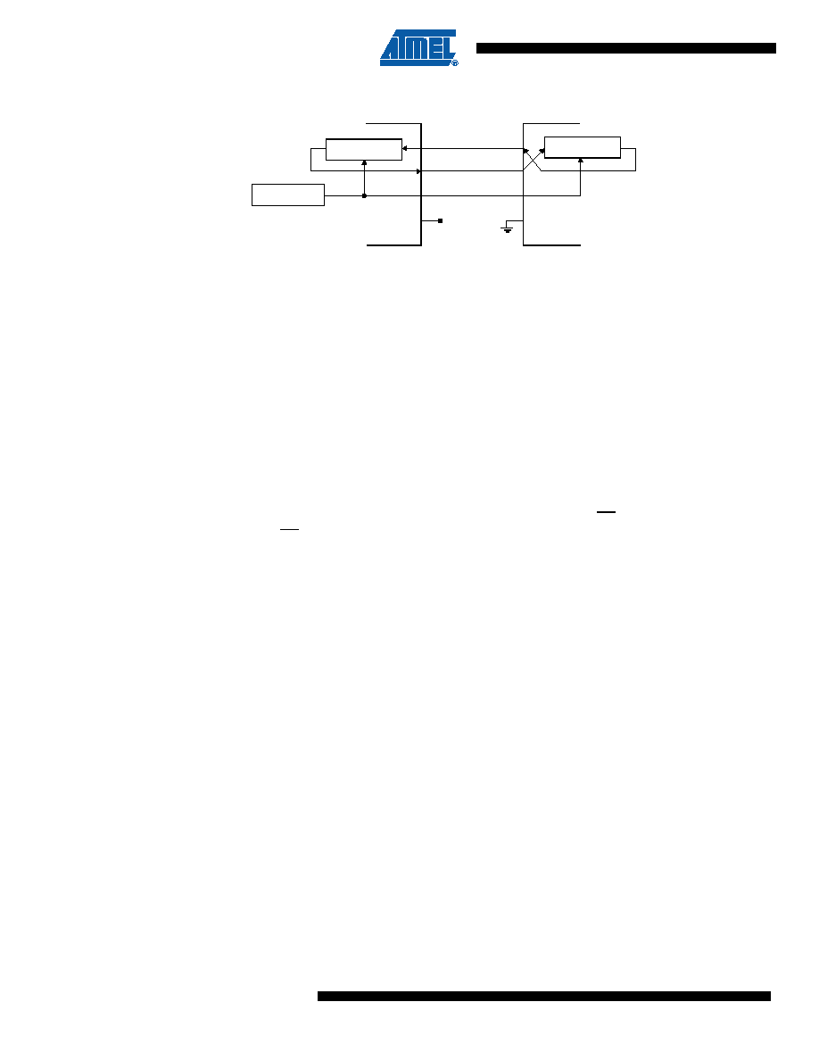
Figure 16-3. Full-Duplex Master-Slave Interconnection
16.3.1.1
Master Mode
The SPI operates in Master mode when the Master bit, MSTR (1), in the SPCON register is set.
Only one Master SPI device can initiate transmissions. Software begins the transmission from a
Master SPI Module by writing to the Serial Peripheral Data Register (SPDAT). If the shift register
is empty, the Byte is immediately transferred to the shift register. The Byte begins shifting out on
MOSI pin under the control of the serial clock, SCK. Simultaneously, another Byte shifts in from
the Slave on the Master’s MISO pin. The transmission ends when the Serial Peripheral transfer
data flag, SPIF, in SPSTA becomes set. At the same time that SPIF becomes set, the received
Byte from the Slave is transferred to the receive data register in SPDAT. Software clears SPIF
by reading the Serial Peripheral Status register (SPSTA) with the SPIF bit set, and then reading
the SPDAT.
16.3.1.2
Slave Mode
The SPI operates in Slave mode when the Master bit, MSTR (2), in the SPCON register is
cleared. Before a data transmission occurs, the Slave Select pin, SS, of the Slave device must
be set to ’0’. SS must remain low until the transmission is complete.
In a Slave SPI Module, data enters the shift register under the control of the SCK from the Mas-
ter SPI Module. After a Byte enters the shift register, it is immediately transferred to the receive
data register in SPDAT, and the SPIF bit is set. To prevent an overflow condition, Slave software
must then read the SPDAT before another Byte enters the shift register (3). A Slave SPI must
complete the write to the SPDAT (shift register) at least one bus cycle before the Master SPI
starts a transmission. If the write to the data register is late, the SPI transmits the data already in
the shift register from the previous transmission. The maximum SCK frequency allowed in slave
mode is F
CLK PERIPH /4.
16.3.2
Transmission Formats
Software can select any of four combinations of serial clock (SCK) phase and polarity using two
bits in the SPCON: the Clock Polarity (CPOL (4)) and the Clock Phase (CPHA4). CPOL defines
the default SCK line level in idle state. It has no significant effect on the transmission format.
CPHA defines the edges on which the input data are sampled and the edges on which the out-
put data are shifted (Figure 16-4 and Figure 16-5). The clock phase and polarity should be
identical for the Master SPI device and the communicating Slave device.
8-bit Shift register
SPI
Clock Generator
Master MCU
8-bit Shift register
MISO
MOSI
SCK
VSS
VDD
SS
Slave MCU
1.
The SPI Module should be configured as a Master before it is enabled (SPEN set). Also, the Mas-
ter SPI should be configured before the Slave SPI.
2.
The SPI Module should be configured as a Slave before it is enabled (SPEN set).
3.
The maximum frequency of the SCK for an SPI configured as a Slave is the bus clock speed.
4.
Before writing to the CPOL and CPHA bits, the SPI should be disabled (SPEN = ’0’).
相关PDF资料 |
PDF描述 |
|---|---|
| REC6-0509SRW/R8/A/X1 | CONV DC/DC 6W 4.5-9VIN 09VOUT |
| ICA-308-SST-H | IC SOCKET 8POS DIP |
| P51-500-S-S-I12-5V-000-000 | SENSOR 500PSIS 1/4 NPT 5V 12" |
| REC3-2412SRW/H6/A/SMD | CONV DC/DC 3W 18-36VIN 12VOUT |
| P51-300-S-S-I12-5V-000-000 | SENSOR 300PSIS 1/4 NPT 5V 12" |
相关代理商/技术参数 |
参数描述 |
|---|---|
| dsPIC33FJ256MC710A-E/PF | 功能描述:数字信号处理器和控制器 - DSP, DSC 16Bit 40MIPS 256KB Flash RoHS:否 制造商:Microchip Technology 核心:dsPIC 数据总线宽度:16 bit 程序存储器大小:16 KB 数据 RAM 大小:2 KB 最大时钟频率:40 MHz 可编程输入/输出端数量:35 定时器数量:3 设备每秒兆指令数:50 MIPs 工作电源电压:3.3 V 最大工作温度:+ 85 C 封装 / 箱体:TQFP-44 安装风格:SMD/SMT |
| dsPIC33FJ256MC710A-E/PT | 功能描述:数字信号处理器和控制器 - DSP, DSC 16Bit 40MIPS 256KB Flash RoHS:否 制造商:Microchip Technology 核心:dsPIC 数据总线宽度:16 bit 程序存储器大小:16 KB 数据 RAM 大小:2 KB 最大时钟频率:40 MHz 可编程输入/输出端数量:35 定时器数量:3 设备每秒兆指令数:50 MIPs 工作电源电压:3.3 V 最大工作温度:+ 85 C 封装 / 箱体:TQFP-44 安装风格:SMD/SMT |
| dsPIC33FJ256MC710A-H/PF | 功能描述:数字信号处理器和控制器 - DSP, DSC 16B MCU 40MIPS 256KB FLASH RoHS:否 制造商:Microchip Technology 核心:dsPIC 数据总线宽度:16 bit 程序存储器大小:16 KB 数据 RAM 大小:2 KB 最大时钟频率:40 MHz 可编程输入/输出端数量:35 定时器数量:3 设备每秒兆指令数:50 MIPs 工作电源电压:3.3 V 最大工作温度:+ 85 C 封装 / 箱体:TQFP-44 安装风格:SMD/SMT |
| dsPIC33FJ256MC710A-H/PT | 功能描述:数字信号处理器和控制器 - DSP, DSC 16B MCU 40MIPS 256KB FLASH RoHS:否 制造商:Microchip Technology 核心:dsPIC 数据总线宽度:16 bit 程序存储器大小:16 KB 数据 RAM 大小:2 KB 最大时钟频率:40 MHz 可编程输入/输出端数量:35 定时器数量:3 设备每秒兆指令数:50 MIPs 工作电源电压:3.3 V 最大工作温度:+ 85 C 封装 / 箱体:TQFP-44 安装风格:SMD/SMT |
| DSPIC33FJ256MC710A-I/P | 制造商:Microchip Technology Inc 功能描述:DSP, Motor Control:Flash Memory, 16-Bit, 40MIPS, 30750 RAM Bytes, TQFP-100 |
发布紧急采购,3分钟左右您将得到回复。