- 您现在的位置:买卖IC网 > PDF目录21335 > DSPIC33FJ32GP204T-I/ML (Microchip Technology)IC DSPIC MCU/DSP 32K 44QFN PDF资料下载
参数资料
| 型号: | DSPIC33FJ32GP204T-I/ML |
| 厂商: | Microchip Technology |
| 文件页数: | 173/176页 |
| 文件大小: | 0K |
| 描述: | IC DSPIC MCU/DSP 32K 44QFN |
| 产品培训模块: | Asynchronous Stimulus |
| 标准包装: | 1,600 |
| 系列: | dsPIC™ 33F |
| 核心处理器: | dsPIC |
| 芯体尺寸: | 16-位 |
| 速度: | 40 MIP |
| 连通性: | I²C,IrDA,LIN,SPI,UART/USART |
| 外围设备: | 欠压检测/复位,POR,PWM,WDT |
| 输入/输出数: | 35 |
| 程序存储器容量: | 32KB(32K x 8) |
| 程序存储器类型: | 闪存 |
| RAM 容量: | 2K x 8 |
| 电压 - 电源 (Vcc/Vdd): | 3 V ~ 3.6 V |
| 数据转换器: | A/D 13x12b |
| 振荡器型: | 内部 |
| 工作温度: | -40°C ~ 85°C |
| 封装/外壳: | 44-VQFN 裸露焊盘 |
| 包装: | 带卷 (TR) |
| 配用: | DV164033-ND - KIT START EXPLORER 16 MPLAB ICD2 DM240001-ND - BOARD DEMO PIC24/DSPIC33/PIC32 |
| 其它名称: | DSPIC33FJ32GP204T-I/MLTR |
第1页第2页第3页第4页第5页第6页第7页第8页第9页第10页第11页第12页第13页第14页第15页第16页第17页第18页第19页第20页第21页第22页第23页第24页第25页第26页第27页第28页第29页第30页第31页第32页第33页第34页第35页第36页第37页第38页第39页第40页第41页第42页第43页第44页第45页第46页第47页第48页第49页第50页第51页第52页第53页第54页第55页第56页第57页第58页第59页第60页第61页第62页第63页第64页第65页第66页第67页第68页第69页第70页第71页第72页第73页第74页第75页第76页第77页第78页第79页第80页第81页第82页第83页第84页第85页第86页第87页第88页第89页第90页第91页第92页第93页第94页第95页第96页第97页第98页第99页第100页第101页第102页第103页第104页第105页第106页第107页第108页第109页第110页第111页第112页第113页第114页第115页第116页第117页第118页第119页第120页第121页第122页第123页第124页第125页第126页第127页第128页第129页第130页第131页第132页第133页第134页第135页第136页第137页第138页第139页第140页第141页第142页第143页第144页第145页第146页第147页第148页第149页第150页第151页第152页第153页第154页第155页第156页第157页第158页第159页第160页第161页第162页第163页第164页第165页第166页第167页第168页第169页第170页第171页第172页当前第173页第174页第175页第176页
95
AT89C5131
4136C–USB–04/05
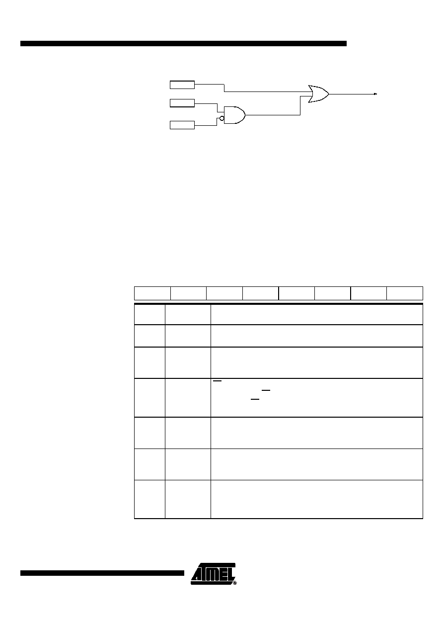
Figure 45. SPI Interrupt Requests Generation
Registers
There are three registers in the module that provide control, status and data storage
functions. These registers are describes in the following paragraphs.
Serial Peripheral Control
Register (SPCON)
The Serial Peripheral Control Register does the following:
–
Selects one of the Master clock rates
–
Configure the SPI module as Master or Slave
–
Selects serial clock polarity and phase
–
Enables the SPI module
–
Frees the SS pin for a general-purpose
Table 75 describes this register and explains the use of each bit.
SSDIS
MODF
CPU Interrupt Request
SPI Receiver/Error
CPU Interrupt Request
SPI Transmitter
SPI
CPU Interrupt Request
SPIF
Table 75. SPCON Register
SPCON - Serial Peripheral Control Register (0C3H)
7654
3210
SPR2
SPEN
SSDIS
MSTR
CPOL
CPHA
SPR1
SPR0
Bit
Number
Bit Mnemonic
Description
7SPR2
Serial Peripheral Rate 2
Bit with SPR1 and SPR0 define the clock rate.
6
SPEN
Serial Peripheral Enable
Cleared to disable the SPI interface.
Set to enable the SPI interface.
5SSDIS
SS Disable
Cleared to enable SS in both Master and Slave modes.
Set to disable SS in both Master and Slave modes. In Slave mode, this bit has
no effect if CPHA = “0”.
5MSTR
Serial Peripheral Master
Cleared to configure the SPI as a Slave.
Set to configure the SPI as a Master.
4CPOL
Clock Polarity
Cleared to have the SCK set to “0” in idle state.
Set to have the SCK set to “1” in idle state.
3CPHA
Clock Phase
Cleared to have the data sampled when the SCK leaves the idle state (see
CPOL).
Set to have the data sampled when the SCK returns to idle state (see CPOL).
相关PDF资料 |
PDF描述 |
|---|---|
| P51-1000-A-T-D-4.5OVP-000-000 | SENSOR 1000PSI 7/16-20-2B 4.5V |
| P51-75-S-I-P-20MA-000-000 | SENSOR 75PSIS 7/16 UNF 4-20MA |
| REC5-483.3SRWZ/H2/A/CTRL | CONV DC/DC 5W 18-72VIN 3.3VOUT |
| P51-200-A-Z-D-4.5V-000-000 | SENSOR 200PSI 1/4-18NPT .5-4.5V |
| P51-15-G-UCF-MD-5V-000-000 | SENSOR 15PSI 9/16-18UNF 1-5V |
相关代理商/技术参数 |
参数描述 |
|---|---|
| dsPIC33FJ32GP302-E/MM | 功能描述:数字信号处理器和控制器 - DSP, DSC 16B MCU/DSP 28 LD 40MIPS 32 KB FLASH RoHS:否 制造商:Microchip Technology 核心:dsPIC 数据总线宽度:16 bit 程序存储器大小:16 KB 数据 RAM 大小:2 KB 最大时钟频率:40 MHz 可编程输入/输出端数量:35 定时器数量:3 设备每秒兆指令数:50 MIPs 工作电源电压:3.3 V 最大工作温度:+ 85 C 封装 / 箱体:TQFP-44 安装风格:SMD/SMT |
| dsPIC33FJ32GP302-E/SO | 功能描述:数字信号处理器和控制器 - DSP, DSC 16B DSC 28LD32KB DMA 40MIPS RoHS:否 制造商:Microchip Technology 核心:dsPIC 数据总线宽度:16 bit 程序存储器大小:16 KB 数据 RAM 大小:2 KB 最大时钟频率:40 MHz 可编程输入/输出端数量:35 定时器数量:3 设备每秒兆指令数:50 MIPs 工作电源电压:3.3 V 最大工作温度:+ 85 C 封装 / 箱体:TQFP-44 安装风格:SMD/SMT |
| dsPIC33FJ32GP302-E/SP | 功能描述:数字信号处理器和控制器 - DSP, DSC 16B DSC 28LD32KB DMA 40MIPS RoHS:否 制造商:Microchip Technology 核心:dsPIC 数据总线宽度:16 bit 程序存储器大小:16 KB 数据 RAM 大小:2 KB 最大时钟频率:40 MHz 可编程输入/输出端数量:35 定时器数量:3 设备每秒兆指令数:50 MIPs 工作电源电压:3.3 V 最大工作温度:+ 85 C 封装 / 箱体:TQFP-44 安装风格:SMD/SMT |
| dsPIC33FJ32GP302-I/MM | 功能描述:数字信号处理器和控制器 - DSP, DSC 16B MCU/DSP 28 LD 40MIPS 32 KB FLASH RoHS:否 制造商:Microchip Technology 核心:dsPIC 数据总线宽度:16 bit 程序存储器大小:16 KB 数据 RAM 大小:2 KB 最大时钟频率:40 MHz 可编程输入/输出端数量:35 定时器数量:3 设备每秒兆指令数:50 MIPs 工作电源电压:3.3 V 最大工作温度:+ 85 C 封装 / 箱体:TQFP-44 安装风格:SMD/SMT |
| dsPIC33FJ32GP302-I/SO | 功能描述:数字信号处理器和控制器 - DSP, DSC 16B DSC 28LD32KB DMA 40MIPS RoHS:否 制造商:Microchip Technology 核心:dsPIC 数据总线宽度:16 bit 程序存储器大小:16 KB 数据 RAM 大小:2 KB 最大时钟频率:40 MHz 可编程输入/输出端数量:35 定时器数量:3 设备每秒兆指令数:50 MIPs 工作电源电压:3.3 V 最大工作温度:+ 85 C 封装 / 箱体:TQFP-44 安装风格:SMD/SMT |
发布紧急采购,3分钟左右您将得到回复。