- 您现在的位置:买卖IC网 > PDF目录3850 > DSPIC33FJ32MC202-I/SS (Microchip Technology)IC DSPIC MCU/DSP 32K 28SSOP PDF资料下载
参数资料
| 型号: | DSPIC33FJ32MC202-I/SS |
| 厂商: | Microchip Technology |
| 文件页数: | 53/76页 |
| 文件大小: | 0K |
| 描述: | IC DSPIC MCU/DSP 32K 28SSOP |
| 标准包装: | 47 |
| 系列: | dsPIC™ 33F |
| 核心处理器: | dsPIC |
| 芯体尺寸: | 16-位 |
| 速度: | 40 MIP |
| 连通性: | I²C,IrDA,LIN,SPI,UART/USART |
| 外围设备: | 欠压检测/复位,DMA,电机控制 PWM,QEI,POR,PWM,WDT |
| 输入/输出数: | 21 |
| 程序存储器容量: | 32KB(32K x 8) |
| 程序存储器类型: | 闪存 |
| RAM 容量: | 2K x 8 |
| 电压 - 电源 (Vcc/Vdd): | 3 V ~ 3.6 V |
| 数据转换器: | A/D 6x10b/12b |
| 振荡器型: | 内部 |
| 工作温度: | -40°C ~ 85°C |
| 封装/外壳: | 28-SSOP(0.209",5.30mm 宽) |
| 包装: | 管件 |
第1页第2页第3页第4页第5页第6页第7页第8页第9页第10页第11页第12页第13页第14页第15页第16页第17页第18页第19页第20页第21页第22页第23页第24页第25页第26页第27页第28页第29页第30页第31页第32页第33页第34页第35页第36页第37页第38页第39页第40页第41页第42页第43页第44页第45页第46页第47页第48页第49页第50页第51页第52页当前第53页第54页第55页第56页第57页第58页第59页第60页第61页第62页第63页第64页第65页第66页第67页第68页第69页第70页第71页第72页第73页第74页第75页第76页
2007-2012 Microchip Technology Inc.
DS70283K-page 57
dsPIC33FJ32MC202/204 and dsPIC33FJ16MC304
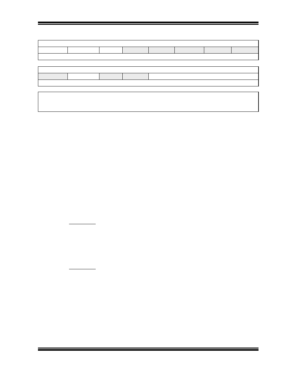
REGISTER 5-1:
NVMCON: FLASH MEMORY CONTROL REGISTER
R/SO-0(1)
R/W-0(1)
U-0
WR
WREN
WRERR
—
bit 15
bit 8
U-0
R/W-0(1)
U-0
R/W-0(1)
—
ERASE
—
—NVMOP<3:0>(2)
bit 7
bit 0
Legend:
SO = Settable Only bit
R = Readable bit
W = Writable bit
U = Unimplemented bit, read as ‘0’
-n = Value at POR
‘1’ = Bit is set
‘0’ = Bit is cleared
x = Bit is unknown
bit 15
WR: Write Control bit
1 = Initiates a Flash memory program or erase operation. The operation is self-timed and the bit is
cleared by hardware once operation is complete
0 = Program or erase operation is complete and inactive
bit 14
WREN: Write Enable bit
1 = Enable Flash program/erase operations
0 = Inhibit Flash program/erase operations
bit 13
WRERR: Write Sequence Error Flag bit
1 = An improper program or erase sequence attempt or termination has occurred (bit is set
automatically on any set attempt of the WR bit)
0 = The program or erase operation completed normally
bit 12-7
Unimplemented: Read as ‘0’
bit 6
ERASE: Erase/Program Enable bit
1 = Perform the erase operation specified by NVMOP<3:0> on the next WR command
0 = Perform the program operation specified by NVMOP<3:0> on the next WR command
bit 5-4
Unimplemented: Read as ‘0’
bit 3-0
NVMOP<3:0>: NVM Operation Select bits(2)
If ERASE = 1:
1111 = Memory bulk erase operation
1101 = Erase General Segment
1100 = Erase Secure Segment
0011 = No operation
0010 = Memory page erase operation
0001 = No operation
0000 = Erase a single Configuration register byte
If ERASE = 0:
1111 = No operation
1101 = No operation
1100 = No operation
0011 = Memory word program operation
0010 = No operation
0001 = Memory row program operation
0000 = Program a single Configuration register byte
Note 1: These bits can only be Reset on a POR.
2: All other combinations of NVMOP<3:0> are unimplemented.
相关PDF资料 |
PDF描述 |
|---|---|
| PIC18LF46J13-I/ML | IC PIC MCU 64KB FLASH 44QFN |
| 52892-1890 | CONN FFC 18POS .50MM R/A ZIF SMD |
| AT89C51RC2-RLTIM | IC 8051 MCU FLASH 32K 44VQFP |
| AT89C51RC2-3CSIM | IC 8051 MCU FLASH 32K 40DIP |
| AT89C51RB2-SLSIM | IC 8051 MCU FLASH 16K 44PLCC |
相关代理商/技术参数 |
参数描述 |
|---|---|
| DSPIC33FJ32MC202T-E/MM | 制造商:Microchip Technology Inc 功能描述:dsPIC33F Series 2 kB RAM 32 kB Flash 16-Bit Digital Signal Controller - QFN-S28 |
| dsPIC33FJ32MC202T-I/MM | 功能描述:数字信号处理器和控制器 - DSP, DSC 16B DSC 28LD32KB Motor40 MIPS RoHS:否 制造商:Microchip Technology 核心:dsPIC 数据总线宽度:16 bit 程序存储器大小:16 KB 数据 RAM 大小:2 KB 最大时钟频率:40 MHz 可编程输入/输出端数量:35 定时器数量:3 设备每秒兆指令数:50 MIPs 工作电源电压:3.3 V 最大工作温度:+ 85 C 封装 / 箱体:TQFP-44 安装风格:SMD/SMT |
| dsPIC33FJ32MC202T-I/SO | 功能描述:数字信号处理器和控制器 - DSP, DSC 16B DSC 28LD32KB Motor40 MIPS RoHS:否 制造商:Microchip Technology 核心:dsPIC 数据总线宽度:16 bit 程序存储器大小:16 KB 数据 RAM 大小:2 KB 最大时钟频率:40 MHz 可编程输入/输出端数量:35 定时器数量:3 设备每秒兆指令数:50 MIPs 工作电源电压:3.3 V 最大工作温度:+ 85 C 封装 / 箱体:TQFP-44 安装风格:SMD/SMT |
| dsPIC33FJ32MC202T-I/SS | 功能描述:数字信号处理器和控制器 - DSP, DSC 16 bit DSC 40MIPS 32KB Flash RoHS:否 制造商:Microchip Technology 核心:dsPIC 数据总线宽度:16 bit 程序存储器大小:16 KB 数据 RAM 大小:2 KB 最大时钟频率:40 MHz 可编程输入/输出端数量:35 定时器数量:3 设备每秒兆指令数:50 MIPs 工作电源电压:3.3 V 最大工作温度:+ 85 C 封装 / 箱体:TQFP-44 安装风格:SMD/SMT |
| dsPIC33FJ32MC204-E/ML | 功能描述:数字信号处理器和控制器 - DSP, DSC 16B DSC 44LD32KB Motor40 MIPS RoHS:否 制造商:Microchip Technology 核心:dsPIC 数据总线宽度:16 bit 程序存储器大小:16 KB 数据 RAM 大小:2 KB 最大时钟频率:40 MHz 可编程输入/输出端数量:35 定时器数量:3 设备每秒兆指令数:50 MIPs 工作电源电压:3.3 V 最大工作温度:+ 85 C 封装 / 箱体:TQFP-44 安装风格:SMD/SMT |
发布紧急采购,3分钟左右您将得到回复。