- 您现在的位置:买卖IC网 > PDF目录11428 > DSPIC33FJ32MC204-E/PT (Microchip Technology)IC DSPIC MCU/DSP 32K 44TQFP PDF资料下载
参数资料
| 型号: | DSPIC33FJ32MC204-E/PT |
| 厂商: | Microchip Technology |
| 文件页数: | 17/76页 |
| 文件大小: | 0K |
| 描述: | IC DSPIC MCU/DSP 32K 44TQFP |
| 产品培训模块: | Asynchronous Stimulus |
| 标准包装: | 160 |
| 系列: | dsPIC™ 33F |
| 核心处理器: | dsPIC |
| 芯体尺寸: | 16-位 |
| 速度: | 40 MIP |
| 连通性: | I²C,IrDA,LIN,SPI,UART/USART |
| 外围设备: | 欠压检测/复位,DMA,电机控制 PWM,QEI,POR,PWM,WDT |
| 输入/输出数: | 35 |
| 程序存储器容量: | 32KB(32K x 8) |
| 程序存储器类型: | 闪存 |
| RAM 容量: | 2K x 8 |
| 电压 - 电源 (Vcc/Vdd): | 3 V ~ 3.6 V |
| 数据转换器: | A/D 9x10b/12b |
| 振荡器型: | 内部 |
| 工作温度: | -40°C ~ 125°C |
| 封装/外壳: | 44-TQFP |
| 包装: | 托盘 |
| 配用: | DV164033-ND - KIT START EXPLORER 16 MPLAB ICD2 DM240001-ND - BOARD DEMO PIC24/DSPIC33/PIC32 |
第1页第2页第3页第4页第5页第6页第7页第8页第9页第10页第11页第12页第13页第14页第15页第16页当前第17页第18页第19页第20页第21页第22页第23页第24页第25页第26页第27页第28页第29页第30页第31页第32页第33页第34页第35页第36页第37页第38页第39页第40页第41页第42页第43页第44页第45页第46页第47页第48页第49页第50页第51页第52页第53页第54页第55页第56页第57页第58页第59页第60页第61页第62页第63页第64页第65页第66页第67页第68页第69页第70页第71页第72页第73页第74页第75页第76页
dsPIC33FJ32MC202/204 and dsPIC33FJ16MC304
DS70283K-page 24
2007-2012 Microchip Technology Inc.
3.6
Arithmetic Logic Unit (ALU)
The dsPIC33FJ32MC202/204 and dsPIC33FJ16MC304
ALU is 16 bits wide and is capable of addition, subtraction,
bit shifts and logic operations. Unless otherwise
mentioned, arithmetic operations are 2’s complement in
nature. Depending on the operation, the ALU can affect
the values of the Carry (C), Zero (Z), Negative (N),
Overflow (OV) and Digit Carry (DC) Status bits in the SR
register. The C and DC Status bits operate as Borrow and
Digit Borrow bits, respectively, for subtraction operations.
The ALU can perform 8-bit or 16-bit operations,
depending on the mode of the instruction that is used.
Data for the ALU operation can come from the W
register array or data memory, depending on the
addressing mode of the instruction. Likewise, output
data from the ALU can be written to the W register array
or a data memory location.
Refer to the “16-bit MCU and DSC Programmer’s Ref-
erence Manual” (DS70157) for information on the SR
bits affected by each instruction.
The dsPIC33FJ32MC202/204 and dsPIC33FJ16MC304
CPU
incorporates
hardware
support
for
both
multiplication and division. This includes a dedicated
hardware
multiplier
and
support
hardware
for
16-bit-divisor division.
3.6.1
MULTIPLIER
Using the high-speed 17-bit x 17-bit multiplier of the
DSP engine, the ALU supports unsigned, signed or
mixed-sign operation in several MCU multiplication
modes:
16-bit x 16-bit signed
16-bit x 16-bit unsigned
16-bit signed x 5-bit (literal) unsigned
16-bit unsigned x 16-bit unsigned
16-bit unsigned x 5-bit (literal) unsigned
16-bit unsigned x 16-bit signed
8-bit unsigned x 8-bit unsigned
3.6.2
DIVIDER
The divide block supports 32-bit/16-bit and 16-bit/16-bit
signed and unsigned integer divide operations with the
following data sizes:
1.
32-bit signed/16-bit signed divide
2.
32-bit unsigned/16-bit unsigned divide
3.
16-bit signed/16-bit signed divide
4.
16-bit unsigned/16-bit unsigned divide
The quotient for all divide instructions ends up in W0
and the remainder in W1. 16-bit signed and unsigned
DIV instructions can specify any W register for both the
16-bit divisor (Wn) and any W register (aligned) pair
(W(m + 1):Wm) for the 32-bit dividend. The divide
algorithm takes one cycle per bit of divisor, so both
32-bit/16-bit and 16-bit/16-bit instructions take the
same number of cycles to execute.
3.7
DSP Engine
The DSP engine consists of a high-speed 17-bit x
17-bit multiplier, a barrel shifter and a 40-bit
adder/subtracter (with two target accumulators, round
and saturation logic).
The dsPIC33FJ32MC202/204 and dsPIC33FJ16MC304
is a single-cycle instruction flow architecture; therefore,
concurrent operation of the DSP engine with MCU
instruction flow is not possible. However, some MCU ALU
and DSP engine resources can be used concurrently by
the same instruction (e.g., ED, EDAC).
The DSP engine can also perform inherent accumula-
tor-to-accumulator operations that require no additional
data. These instructions are ADD, SUB and NEG.
The DSP engine has options selected through bits in
the CPU Core Control register (CORCON), as listed
below:
Fractional or integer DSP multiply (IF)
Signed or unsigned DSP multiply (US)
Conventional or convergent rounding (RND)
Automatic saturation on/off for ACCA (SATA)
Automatic saturation on/off for ACCB (SATB)
Automatic saturation on/off for writes to data
memory (SATDW)
Accumulator Saturation mode selection (ACCSAT)
A block diagram of the DSP engine is shown in
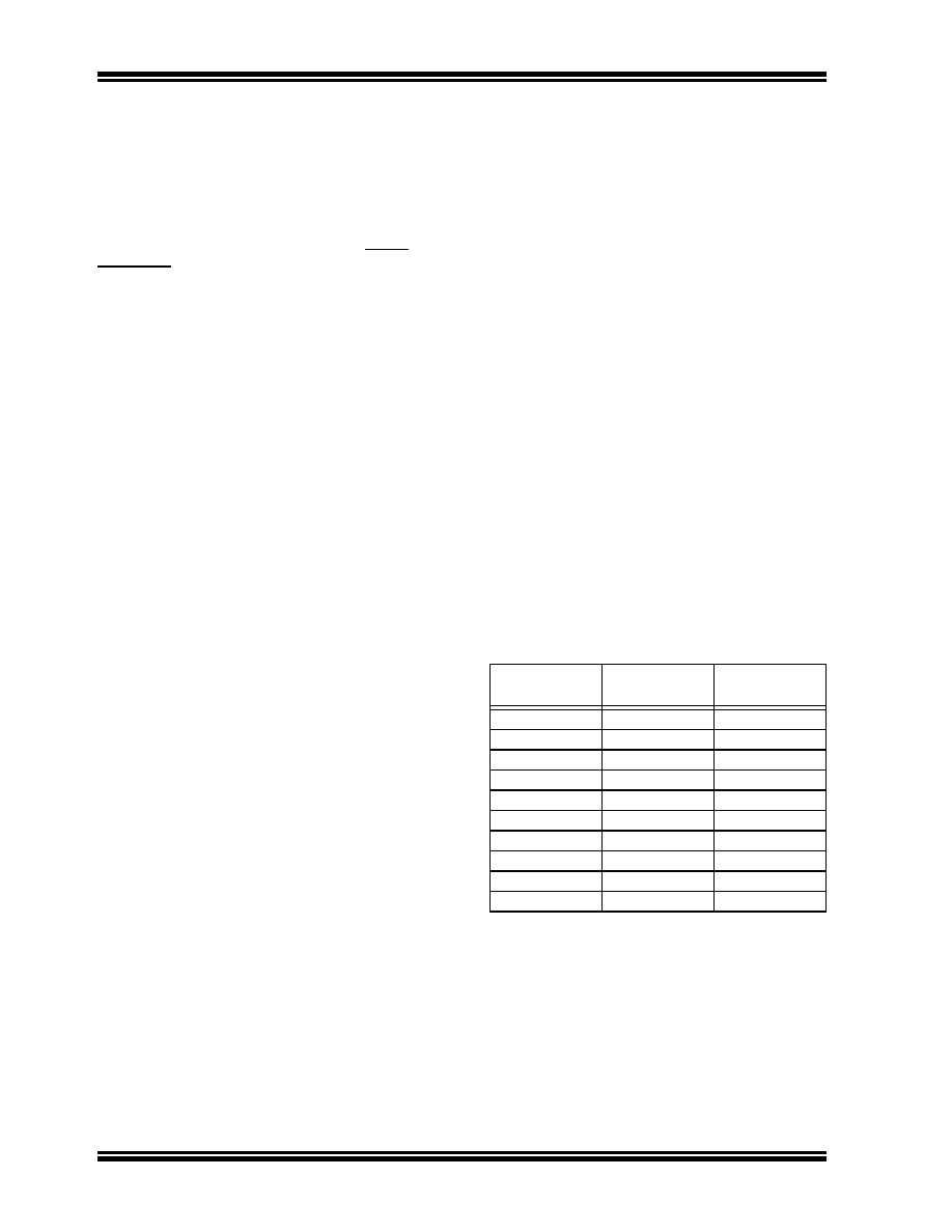
TABLE 3-1:
DSP INSTRUCTIONS
SUMMARY
Instruction
Algebraic
Operation
ACC Write
Back
CLR
A = 0
Yes
ED
A = (x - y)2
No
EDAC
A = A + (x – y)2
No
MAC
A = A + (x * y)
Yes
MAC
A = A + x2
No
MOVSAC
No change in A
Yes
MPY
A = x y
No
MPY
A = x2
No
MPY.N
A = – x y
No
MSC
A = A – x y
Yes
相关PDF资料 |
PDF描述 |
|---|---|
| PIC16C62BT-20I/SS | IC MCU OTP 2KX14 PWM 28SSOP |
| VI-23W-CV-F3 | CONVERTER MOD DC/DC 5.5V 150W |
| HR25A-7P-4S | CONN PLUG 4POS FEMALE CIRCULAR |
| PIC32MX250F128B-V/ML | IC MCU 32BIT 128KB FLASH 28QFN |
| ISL54406IRTZ-T | IC SWITCH DUAL SPST 10-TDFN |
相关代理商/技术参数 |
参数描述 |
|---|---|
| dsPIC33FJ32MC204-H/ML | 功能描述:数字信号处理器和控制器 - DSP, DSC 16-bit 32KB Flash 40 MIPS RoHS:否 制造商:Microchip Technology 核心:dsPIC 数据总线宽度:16 bit 程序存储器大小:16 KB 数据 RAM 大小:2 KB 最大时钟频率:40 MHz 可编程输入/输出端数量:35 定时器数量:3 设备每秒兆指令数:50 MIPs 工作电源电压:3.3 V 最大工作温度:+ 85 C 封装 / 箱体:TQFP-44 安装风格:SMD/SMT |
| dsPIC33FJ32MC204-H/PT | 功能描述:数字信号处理器和控制器 - DSP, DSC 16-bit 32KB Flash 40 MIPS RoHS:否 制造商:Microchip Technology 核心:dsPIC 数据总线宽度:16 bit 程序存储器大小:16 KB 数据 RAM 大小:2 KB 最大时钟频率:40 MHz 可编程输入/输出端数量:35 定时器数量:3 设备每秒兆指令数:50 MIPs 工作电源电压:3.3 V 最大工作温度:+ 85 C 封装 / 箱体:TQFP-44 安装风格:SMD/SMT |
| dsPIC33FJ32MC204-I/ML | 功能描述:数字信号处理器和控制器 - DSP, DSC 16B DSC 44LD 32KB FlashMotor40 RoHS:否 制造商:Microchip Technology 核心:dsPIC 数据总线宽度:16 bit 程序存储器大小:16 KB 数据 RAM 大小:2 KB 最大时钟频率:40 MHz 可编程输入/输出端数量:35 定时器数量:3 设备每秒兆指令数:50 MIPs 工作电源电压:3.3 V 最大工作温度:+ 85 C 封装 / 箱体:TQFP-44 安装风格:SMD/SMT |
| dsPIC33FJ32MC204-I/PT | 功能描述:数字信号处理器和控制器 - DSP, DSC 16B DSC 44LD 32KB FlashMotor40 RoHS:否 制造商:Microchip Technology 核心:dsPIC 数据总线宽度:16 bit 程序存储器大小:16 KB 数据 RAM 大小:2 KB 最大时钟频率:40 MHz 可编程输入/输出端数量:35 定时器数量:3 设备每秒兆指令数:50 MIPs 工作电源电压:3.3 V 最大工作温度:+ 85 C 封装 / 箱体:TQFP-44 安装风格:SMD/SMT |
| dsPIC33FJ32MC204T-I/ML | 功能描述:数字信号处理器和控制器 - DSP, DSC 16B DSC 44LD32KB Motor40 MIPS RoHS:否 制造商:Microchip Technology 核心:dsPIC 数据总线宽度:16 bit 程序存储器大小:16 KB 数据 RAM 大小:2 KB 最大时钟频率:40 MHz 可编程输入/输出端数量:35 定时器数量:3 设备每秒兆指令数:50 MIPs 工作电源电压:3.3 V 最大工作温度:+ 85 C 封装 / 箱体:TQFP-44 安装风格:SMD/SMT |
发布紧急采购,3分钟左右您将得到回复。