- 您现在的位置:买卖IC网 > PDF目录3869 > DSPIC33FJ64GP710T-I/PF (Microchip Technology)IC DSPIC MCU/DSP 64K 100TQFP PDF资料下载
参数资料
| 型号: | DSPIC33FJ64GP710T-I/PF |
| 厂商: | Microchip Technology |
| 文件页数: | 76/197页 |
| 文件大小: | 0K |
| 描述: | IC DSPIC MCU/DSP 64K 100TQFP |
| 产品培训模块: | Asynchronous Stimulus |
| 标准包装: | 1,000 |
| 系列: | dsPIC™ 33F |
| 核心处理器: | dsPIC |
| 芯体尺寸: | 16-位 |
| 速度: | 40 MIP |
| 连通性: | CAN,I²C,IrDA,LIN,SPI,UART/USART |
| 外围设备: | AC'97,欠压检测/复位,DMA,I²S,POR,PWM,WDT |
| 输入/输出数: | 85 |
| 程序存储器容量: | 64KB(64K x 8) |
| 程序存储器类型: | 闪存 |
| RAM 容量: | 16K x 8 |
| 电压 - 电源 (Vcc/Vdd): | 3 V ~ 3.6 V |
| 数据转换器: | A/D 32x10b/12b |
| 振荡器型: | 内部 |
| 工作温度: | -40°C ~ 85°C |
| 封装/外壳: | 100-TQFP |
| 包装: | 带卷 (TR) |
| 配用: | DM300024-ND - KIT DEMO DSPICDEM 1.1 DV164033-ND - KIT START EXPLORER 16 MPLAB ICD2 MA330012-ND - MODULE DSPIC33 100P TO 84QFP MA330011-ND - MODULE DSPIC33 100P TO 100QFP DM240001-ND - BOARD DEMO PIC24/DSPIC33/PIC32 AC164323-ND - MODULE SKT FOR 100TQFP |
第1页第2页第3页第4页第5页第6页第7页第8页第9页第10页第11页第12页第13页第14页第15页第16页第17页第18页第19页第20页第21页第22页第23页第24页第25页第26页第27页第28页第29页第30页第31页第32页第33页第34页第35页第36页第37页第38页第39页第40页第41页第42页第43页第44页第45页第46页第47页第48页第49页第50页第51页第52页第53页第54页第55页第56页第57页第58页第59页第60页第61页第62页第63页第64页第65页第66页第67页第68页第69页第70页第71页第72页第73页第74页第75页当前第76页第77页第78页第79页第80页第81页第82页第83页第84页第85页第86页第87页第88页第89页第90页第91页第92页第93页第94页第95页第96页第97页第98页第99页第100页第101页第102页第103页第104页第105页第106页第107页第108页第109页第110页第111页第112页第113页第114页第115页第116页第117页第118页第119页第120页第121页第122页第123页第124页第125页第126页第127页第128页第129页第130页第131页第132页第133页第134页第135页第136页第137页第138页第139页第140页第141页第142页第143页第144页第145页第146页第147页第148页第149页第150页第151页第152页第153页第154页第155页第156页第157页第158页第159页第160页第161页第162页第163页第164页第165页第166页第167页第168页第169页第170页第171页第172页第173页第174页第175页第176页第177页第178页第179页第180页第181页第182页第183页第184页第185页第186页第187页第188页第189页第190页第191页第192页第193页第194页第195页第196页第197页
168
AT89C51CC03
4182O–CAN–09/08
Electrical Characteristics
Absolute Maximum Ratings
ICCOP Test Conditions
Power Consumption
Management
Since the introduction of the first C51 device, every manufacturer made operating I
CC
measurements under Reset, which made sense for the designs where the CPU was
running under reset. In our new devices, the CPU is no longer active during reset, so the
power consumption is very low but not representative of what will happen in the cus-
tomer system. Thus, while keeping measurements under Reset, we present a new way
to measure the operating I
CC.
Using an internal test ROM, the following code is executed.
Label: SJMP Label (80FE)
Ports 1 and 4 are disconnected, RST = Vcc, XTAL2 is not connected and XTAL1 is
driven by the clock.
This is much more representative of the real operating Icc.
DC Parameters for Standard Voltage
Industrial T
A = -40°C to +85°C; VSS = 0V;
Automotive T
A = -40°C to +125°C; VSS = 0V
V
CC =3.0V to 5.5V and F = 0 to 40 MHz (both internal and external code execution)
V
CC =4.5V to 5.5V and F = 0 to 60 MHz (internal code execution only)
Ambiant Temperature Under Bias:
I = industrial........................................................-40
°C to 85°C
A = automotive..................................................-40°C to +125°C
Voltage on V
CC from VSS ......................................-0.5V to + 6V
Voltage on Any Pin from VSS..................... -0.5V to VCC + 0.2V
Power Dissipation .............................................................. 1 W
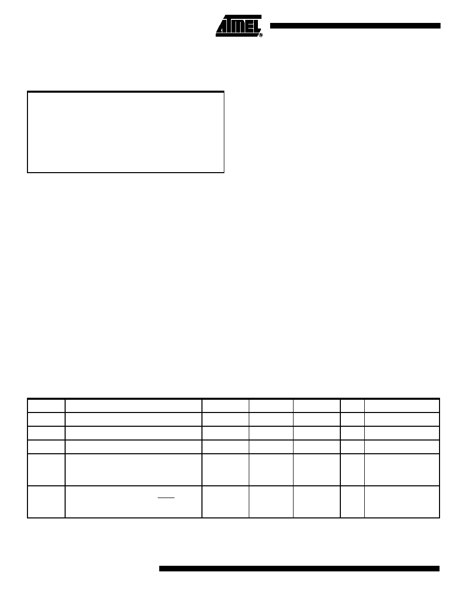
Table 116. DC Parameters in Standard Voltage
Symbol
Parameter
Min
Typ(5)
Max
Unit
Test Conditions
V
IL
Input Low Voltage
-0.5
0.2Vcc - 0.1
V
IH
Input High Voltage except XTAL1, RST
0.2 V
CC + 0.9
V
CC + 0.5
V
VIH1
Input High Voltage, XTAL1, RST
0.7 VCC
VCC + 0.5
V
VOL
Output Low Voltage, ports 1, 2, 3 and 4
(6)
0.3
0.45
1.0
V
IOL = 100 μA
(4)
IOL = 1.6 mA
(4)
IOL = 3.5 mA
(4)
VOL1
Output Low Voltage, port 0, ALE, PSEN
(6)
0.3
0.45
1.0
V
IOL = 200 μA
(4)
IOL = 3.2 mA
(4)
IOL = 7.0 mA
(4)
Note:
Stresses at or above those listed under “Absolute Maximum
Ratings” may cause permanent damage to the device. This
is a stress rating only and functional operation of the device
at these or any other conditions above those indicated in
the operational sections of this specification is not implied.
Exposure to absolute maximum rating conditions may affect
device reliability.
The power dissipation is based on the maximum allowable
die temperature and the thermal resistance of the package.
相关PDF资料 |
PDF描述 |
|---|---|
| PIC16F1939-I/ML | IC MCU 8BIT FLASH 44QFN |
| PIC24FJ64GB108T-I/PT | IC PIC MCU FLASH 80TQFP |
| PIC16LF1946-I/PT | IC MCU 8BIT FLASH 64TQFP |
| PIC24FJ192GB110T-I/PT | IC PIC MCU FLASH 100TQFP |
| PIC24FJ192GB110T-I/PF | IC PIC MCU FLASH 100TQFP |
相关代理商/技术参数 |
参数描述 |
|---|---|
| dsPIC33FJ64GP802-E/MM | 功能描述:数字信号处理器和控制器 - DSP, DSC 16Bit MCU/DSP 40MIPS 64KB FLASH RoHS:否 制造商:Microchip Technology 核心:dsPIC 数据总线宽度:16 bit 程序存储器大小:16 KB 数据 RAM 大小:2 KB 最大时钟频率:40 MHz 可编程输入/输出端数量:35 定时器数量:3 设备每秒兆指令数:50 MIPs 工作电源电压:3.3 V 最大工作温度:+ 85 C 封装 / 箱体:TQFP-44 安装风格:SMD/SMT |
| dsPIC33FJ64GP802-E/SO | 功能描述:数字信号处理器和控制器 - DSP, DSC 16bit DSC 64KB Flash CAN DMA 40MIPS RoHS:否 制造商:Microchip Technology 核心:dsPIC 数据总线宽度:16 bit 程序存储器大小:16 KB 数据 RAM 大小:2 KB 最大时钟频率:40 MHz 可编程输入/输出端数量:35 定时器数量:3 设备每秒兆指令数:50 MIPs 工作电源电压:3.3 V 最大工作温度:+ 85 C 封装 / 箱体:TQFP-44 安装风格:SMD/SMT |
| dsPIC33FJ64GP802-E/SP | 功能描述:数字信号处理器和控制器 - DSP, DSC 16B DSC 28LD64KB DMA 40MIPS RoHS:否 制造商:Microchip Technology 核心:dsPIC 数据总线宽度:16 bit 程序存储器大小:16 KB 数据 RAM 大小:2 KB 最大时钟频率:40 MHz 可编程输入/输出端数量:35 定时器数量:3 设备每秒兆指令数:50 MIPs 工作电源电压:3.3 V 最大工作温度:+ 85 C 封装 / 箱体:TQFP-44 安装风格:SMD/SMT |
| dsPIC33FJ64GP802-H/MM | 功能描述:数字信号处理器和控制器 - DSP, DSC 16-bit 64KB Flash CAN DMA RoHS:否 制造商:Microchip Technology 核心:dsPIC 数据总线宽度:16 bit 程序存储器大小:16 KB 数据 RAM 大小:2 KB 最大时钟频率:40 MHz 可编程输入/输出端数量:35 定时器数量:3 设备每秒兆指令数:50 MIPs 工作电源电压:3.3 V 最大工作温度:+ 85 C 封装 / 箱体:TQFP-44 安装风格:SMD/SMT |
| dsPIC33FJ64GP802-H/SO | 功能描述:数字信号处理器和控制器 - DSP, DSC 16-bit 64KB Flash CAN DMA RoHS:否 制造商:Microchip Technology 核心:dsPIC 数据总线宽度:16 bit 程序存储器大小:16 KB 数据 RAM 大小:2 KB 最大时钟频率:40 MHz 可编程输入/输出端数量:35 定时器数量:3 设备每秒兆指令数:50 MIPs 工作电源电压:3.3 V 最大工作温度:+ 85 C 封装 / 箱体:TQFP-44 安装风格:SMD/SMT |
发布紧急采购,3分钟左右您将得到回复。