- 您现在的位置:买卖IC网 > PDF目录3869 > DSPIC33FJ64MC510T-I/PF (Microchip Technology)IC DSPIC MCU/DSP 64K 100TQFP PDF资料下载
参数资料
| 型号: | DSPIC33FJ64MC510T-I/PF |
| 厂商: | Microchip Technology |
| 文件页数: | 165/199页 |
| 文件大小: | 0K |
| 描述: | IC DSPIC MCU/DSP 64K 100TQFP |
| 产品培训模块: | Asynchronous Stimulus |
| 标准包装: | 1,000 |
| 系列: | dsPIC™ 33F |
| 核心处理器: | dsPIC |
| 芯体尺寸: | 16-位 |
| 速度: | 40 MIP |
| 连通性: | CAN,I²C,IrDA,LIN,SPI,UART/USART |
| 外围设备: | 欠压检测/复位,DMA,电机控制 PWM,QEI,POR,PWM,WDT |
| 输入/输出数: | 85 |
| 程序存储器容量: | 64KB(64K x 8) |
| 程序存储器类型: | 闪存 |
| RAM 容量: | 8K x 8 |
| 电压 - 电源 (Vcc/Vdd): | 3 V ~ 3.6 V |
| 数据转换器: | A/D 24x10b/12b |
| 振荡器型: | 内部 |
| 工作温度: | -40°C ~ 85°C |
| 封装/外壳: | 100-TQFP |
| 包装: | 带卷 (TR) |
| 配用: | MA330013-ND - MODULE PLUG-IN DSPIC33 100TQFP DV164033-ND - KIT START EXPLORER 16 MPLAB ICD2 DM240001-ND - BOARD DEMO PIC24/DSPIC33/PIC32 AC164323-ND - MODULE SKT FOR 100TQFP |
第1页第2页第3页第4页第5页第6页第7页第8页第9页第10页第11页第12页第13页第14页第15页第16页第17页第18页第19页第20页第21页第22页第23页第24页第25页第26页第27页第28页第29页第30页第31页第32页第33页第34页第35页第36页第37页第38页第39页第40页第41页第42页第43页第44页第45页第46页第47页第48页第49页第50页第51页第52页第53页第54页第55页第56页第57页第58页第59页第60页第61页第62页第63页第64页第65页第66页第67页第68页第69页第70页第71页第72页第73页第74页第75页第76页第77页第78页第79页第80页第81页第82页第83页第84页第85页第86页第87页第88页第89页第90页第91页第92页第93页第94页第95页第96页第97页第98页第99页第100页第101页第102页第103页第104页第105页第106页第107页第108页第109页第110页第111页第112页第113页第114页第115页第116页第117页第118页第119页第120页第121页第122页第123页第124页第125页第126页第127页第128页第129页第130页第131页第132页第133页第134页第135页第136页第137页第138页第139页第140页第141页第142页第143页第144页第145页第146页第147页第148页第149页第150页第151页第152页第153页第154页第155页第156页第157页第158页第159页第160页第161页第162页第163页第164页当前第165页第166页第167页第168页第169页第170页第171页第172页第173页第174页第175页第176页第177页第178页第179页第180页第181页第182页第183页第184页第185页第186页第187页第188页第189页第190页第191页第192页第193页第194页第195页第196页第197页第198页第199页
dsPIC33F
DS7
0165E-page
66
P
reli
m
inary
20
07
M
ic
rochip
T
e
c
hnology
In
c
.
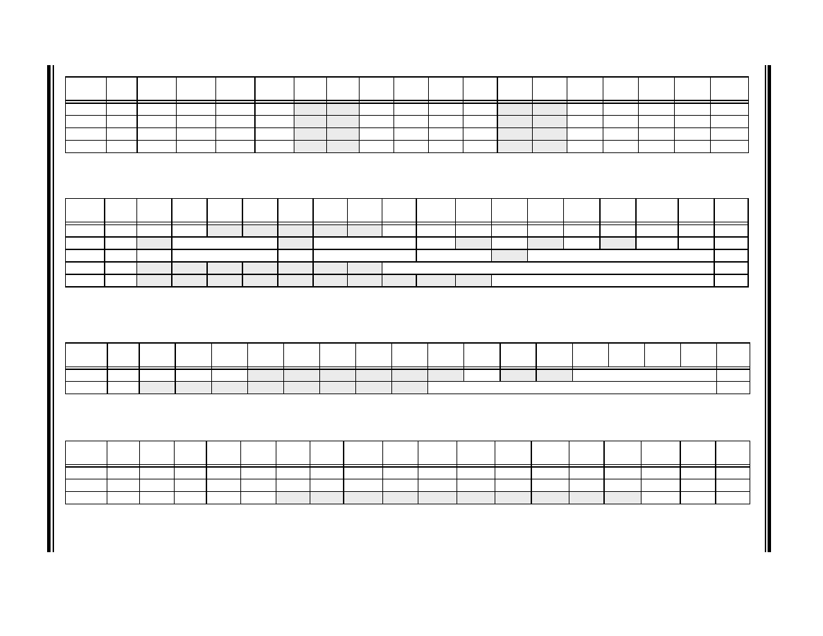
TABLE 3-31:
PORTG REGISTER MAP(1)
File Name
Addr
Bit 15
Bit 14
Bit 13
Bit 12
Bit 11
Bit 10
Bit 9
Bit 8
Bit 7
Bit 6
Bit 5
Bit 4
Bit 3
Bit 2
Bit 1
Bit 0
All
Resets
TRISG
02E4
TRISG15
TRISG14
TRISG13
TRISG12
—
TRISG9
TRISG8
TRISG7
TRISG6
—
TRISG3
TRISG2
TRISG1
TRISG0
F3CF
PORTG
02E6
RG15
RG14
RG13
RG12
—
RG9
RG8
RG7
RG6
—
—RG3
RG2
RG1
RG0
xxxx
LATG
02E8
LATG15
LATG14
LATG13
LATG12
—
LATG9
LATG8
LATG7
LATG6
—
—LATG3
LATG2
LATG1
LATG0
xxxx
ODCG
06E4
ODCG15
ODCG14
ODCG13
ODCG12
—
ODCG9
ODCG8
ODCG7
ODCG6
—
ODCG3
ODCG2
ODCG1
ODCG0
xxxx
Legend:
x
= unknown value on Reset, — = unimplemented, read as ‘0’. Reset values are shown in hexadecimal for 100-pin devices.
Note
1:
The actual set of I/O port pins varies from one device to another. Please refer to the corresponding pinout diagrams.
TABLE 3-32:
SYSTEM CONTROL REGISTER MAP
File Name
Addr
Bit 15
Bit 14
Bit 13
Bit 12
Bit 11
Bit 10
Bit 9
Bit 8
Bit 7
Bit 6
Bit 5
Bit 4
Bit 3
Bit 2
Bit 1
Bit 0
All
Resets
RCON
0740
TRAPR
IOPUWR
—
VREGS
EXTR
SWR
SWDTEN
WDTO
SLEEP
IDLE
BOR
POR
xxxx(1)
OSCCON
0742
—COSC<2:0>
—
NOSC<2:0>
CLKLOCK
—LOCK
—CF
—
LPOSCEN
OSWEN
0300(2)
CLKDIV
0744
ROI
DOZE<2:0>
DOZEN
FRCDIV<2:0>
PLLPOST<1:0>
—
PLLPRE<4::0>
0040
PLLFBD
0746
—
PLLDIV<8:0>
0030
OSCTUN
0748
—
TUN<5:0>
0000
Legend:
x
= unknown value on Reset, — = unimplemented, read as ‘0’. Reset values are shown in hexadecimal.
Note
1:
RCON register Reset values dependent on type of Reset.
2:
OSCCON register Reset values dependent on the FOSC Configuration bits and by type of Reset.
TABLE 3-33:
NVM REGISTER MAP
File Name
Addr
Bit 15
Bit 14
Bit 13
Bit 12
Bit 11
Bit 10
Bit 9
Bit 8
Bit 7
Bit 6
Bit 5
Bit 4
Bit 3
Bit 2
Bit 1
Bit 0
All
Resets
NVMCON
0760
WR
WREN
WRERR
—
ERASE
—
—NVMOP<3:0>
0000
(1)
NVMKEY
0766
—
NVMKEY<7:0>
0000
Legend:
x
= unknown value on Reset, — = unimplemented, read as ‘0’. Reset values are shown in hexadecimal.
Note
1:
Reset value shown is for POR only. Value on other Reset states is dependent on the state of memory write or erase operations at the time of Reset.
TABLE 3-34:
PMD REGISTER MAP
File Name
Addr
Bit 15
Bit 14
Bit 13
Bit 12
Bit 11
Bit 10
Bit 9
Bit 8
Bit 7
Bit 6
Bit 5
Bit 4
Bit 3
Bit 2
Bit 1
Bit 0
All
Resets
PMD1
0770
T5MD
T4MD
T3MD
T2MD
T1MD
QEIMD
PWMMD
DCIMD
I2C1MD
U2MD
U1MD
SPI2MD
SPI1MD
C2MD
C1MD
AD1MD
0000
PMD2
0772
IC8MD
IC7MD
IC6MD
IC5MD
IC4MD
IC3MD
IC2MD
IC1MD
OC8MD
OC7MD
OC6MD
OC5MD
OC4MD
OC3MD
OC2MD
OC1MD
0000
PMD3
0774
T9MD
T8MD
T7MD
T6MD
—
—I2C2MD
AD2MD
0000
Legend:
x
= unknown value on Reset, — = unimplemented, read as ‘0’. Reset values are shown in hexadecimal.
相关PDF资料 |
PDF描述 |
|---|---|
| DSPIC33FJ64GP710T-I/PT | IC DSPIC MCU/DSP 64K 100TQFP |
| DSPIC33FJ64GP710T-I/PF | IC DSPIC MCU/DSP 64K 100TQFP |
| PIC16F1939-I/ML | IC MCU 8BIT FLASH 44QFN |
| PIC24FJ64GB108T-I/PT | IC PIC MCU FLASH 80TQFP |
| PIC16LF1946-I/PT | IC MCU 8BIT FLASH 64TQFP |
相关代理商/技术参数 |
参数描述 |
|---|---|
| dsPIC33FJ64MC706A-E/MR | 功能描述:数字信号处理器和控制器 - DSP, DSC 16 Bit MCU/DSP 64LD 40MIPS 64KB FLASH RoHS:否 制造商:Microchip Technology 核心:dsPIC 数据总线宽度:16 bit 程序存储器大小:16 KB 数据 RAM 大小:2 KB 最大时钟频率:40 MHz 可编程输入/输出端数量:35 定时器数量:3 设备每秒兆指令数:50 MIPs 工作电源电压:3.3 V 最大工作温度:+ 85 C 封装 / 箱体:TQFP-44 安装风格:SMD/SMT |
| dsPIC33FJ64MC706A-E/PT | 功能描述:数字信号处理器和控制器 - DSP, DSC 16Bit 40MIPS 64KB Flash RoHS:否 制造商:Microchip Technology 核心:dsPIC 数据总线宽度:16 bit 程序存储器大小:16 KB 数据 RAM 大小:2 KB 最大时钟频率:40 MHz 可编程输入/输出端数量:35 定时器数量:3 设备每秒兆指令数:50 MIPs 工作电源电压:3.3 V 最大工作温度:+ 85 C 封装 / 箱体:TQFP-44 安装风格:SMD/SMT |
| dsPIC33FJ64MC706A-I/MR | 功能描述:数字信号处理器和控制器 - DSP, DSC 16Bit MCU/DSP 40MIPS 64KB FLASH RoHS:否 制造商:Microchip Technology 核心:dsPIC 数据总线宽度:16 bit 程序存储器大小:16 KB 数据 RAM 大小:2 KB 最大时钟频率:40 MHz 可编程输入/输出端数量:35 定时器数量:3 设备每秒兆指令数:50 MIPs 工作电源电压:3.3 V 最大工作温度:+ 85 C 封装 / 箱体:TQFP-44 安装风格:SMD/SMT |
| dsPIC33FJ64MC706A-I/PT | 功能描述:数字信号处理器和控制器 - DSP, DSC 16Bit 40MIPS 64KB Flash RoHS:否 制造商:Microchip Technology 核心:dsPIC 数据总线宽度:16 bit 程序存储器大小:16 KB 数据 RAM 大小:2 KB 最大时钟频率:40 MHz 可编程输入/输出端数量:35 定时器数量:3 设备每秒兆指令数:50 MIPs 工作电源电压:3.3 V 最大工作温度:+ 85 C 封装 / 箱体:TQFP-44 安装风格:SMD/SMT |
| dsPIC33FJ64MC706AT-I/MR | 功能描述:数字信号处理器和控制器 - DSP, DSC 16 Bit MCU/DSP 64LD 40MIPS 64KB FLASH RoHS:否 制造商:Microchip Technology 核心:dsPIC 数据总线宽度:16 bit 程序存储器大小:16 KB 数据 RAM 大小:2 KB 最大时钟频率:40 MHz 可编程输入/输出端数量:35 定时器数量:3 设备每秒兆指令数:50 MIPs 工作电源电压:3.3 V 最大工作温度:+ 85 C 封装 / 箱体:TQFP-44 安装风格:SMD/SMT |
发布紧急采购,3分钟左右您将得到回复。