- 您现在的位置:买卖IC网 > PDF目录97873 > E4707B-EDGE4707B Quad Channel Per-Pin Precision Measurement Unit PDF资料下载
参数资料
| 型号: | E4707B-EDGE4707B |
| 英文描述: | Quad Channel Per-Pin Precision Measurement Unit |
| 中文描述: | 四通道按针脚精密测量单元 |
| 文件页数: | 2/25页 |
| 文件大小: | 194K |
| 代理商: | E4707B-EDGE4707B |
10
Revision 3 / December 18, 2002
www .semtech.com
TEST AND MEASUREMENT PRODUCTS
Edge4707B
REXT Selection
The Edge 4707B is designed for the voltage drop across
RA, RB, RC, and RD to be
≤ 2V with the maximum current
passing through them.
However, these resistor values
can be changed to support different applications.
Increasing the maximum current beyond the nominal range
is not recommended. However, decreasing the maximum
current is allowed by increasing the external resistor using
the equation IMAX = 2V / REXT.
Switch Operation on Force and Sense Lines
Each channel of the Edge4707B features two switches
connected to the FORCE output pin (External Force = 45
,
Internal Force = 100
) and one 1K switch connected
to the SENSE input pin. These switches are controlled by
the TTL compatible inputs I_FCSEL, E_FCSEL, and
E_SNSEL. Switch operation is described in Table 7.
Table 7.
These switches can be configured to route the Edge4707B
for external forcing or sensing operations (see Figure 2).
For external forcing operation, the switch controlled by
I_FCSEL can be used to internally isolate the PMU from
the FORCE output.
This enables the user to connect
the FORCE pin to an external device connected to the
E_FC_IN pin using the switch controlled by the E_FC_SEL
input. I_FCSEL and E_FCSEL functionality is described in
Table 8.
Circuit Description (continued)
Table 8.
For external sense operation, the switch controlled by
E_SNSEL can be used to internally connect the SENSE
input pin to the E_SN_IN output pin (see Figure 2). This
allows the user to use the E_SN_IN pin for remote sensing.
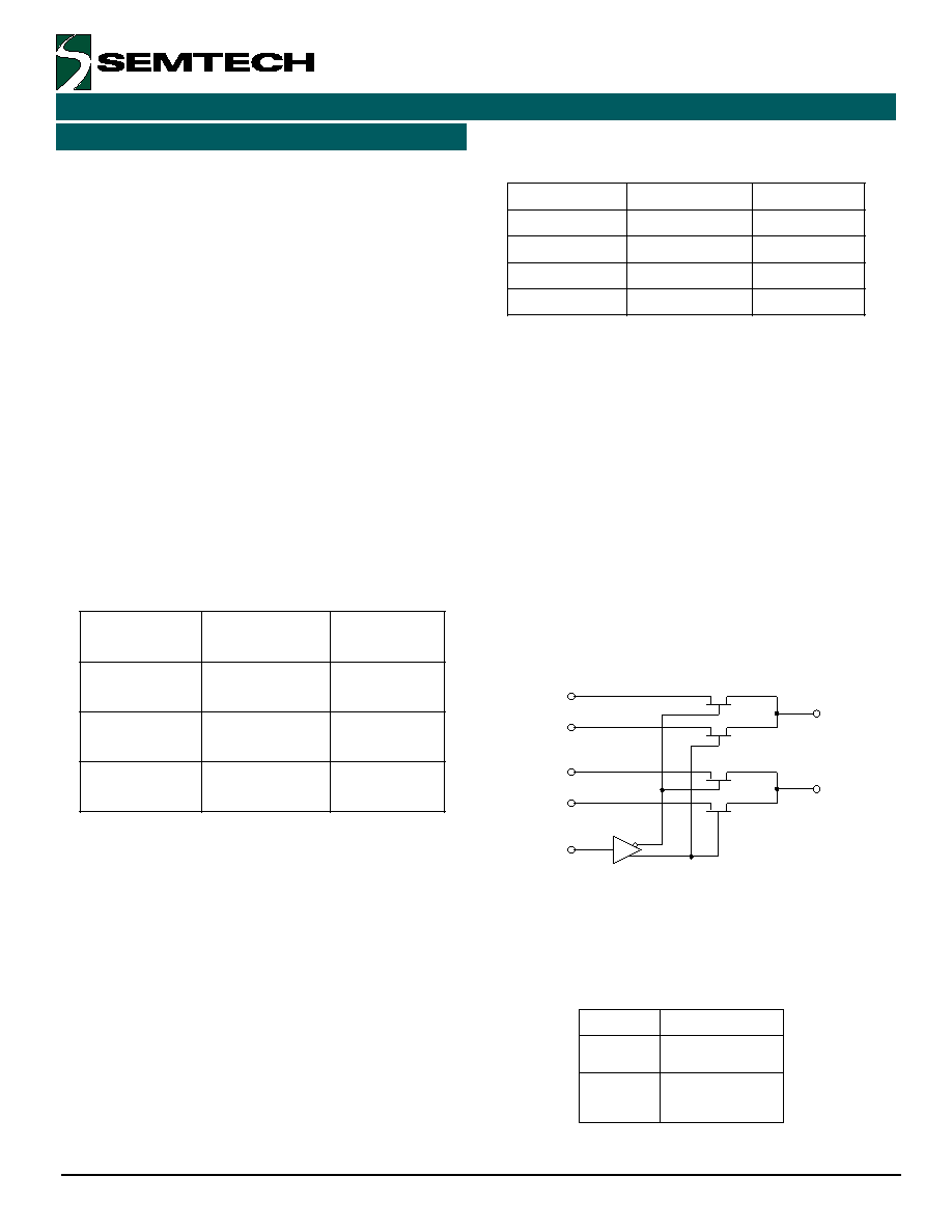
Analog MUX
The Edge4707B has a separate analog mux section which
is intended for 12V flash programming signal muxing with
lower, more standard voltages. There are five inputs for
this section, all of which are brought out to external pins
(see Figure 3). The two outputs, DVH and DVL, connect
to driver reference voltages of the Edge720 (or other pin
electronics drivers).
Figure 3. Analog MUX Section
(Typically used to provide flash programming and standard
voltages to driver pin electronic references.)
The truth table for SV-SEL is shown in Table 9.
Table 9. SV-SEL Truth Table
L
E
S
_
V
S
0
H
I
V
=
H
V
D
L
I
V
=
L
V
D
1
H
I
V
=
H
V
D
H
L
I
V
=
L
V
D
)
e
g
a
t
l
o
v
r
e
p
u
s
(
L
E
S
C
F
_
IL
E
S
C
F
_
EE
C
R
O
F
00
Z
i
H
11
n
o
i
t
i
d
n
o
C
l
a
g
e
l
I
10
P
N
I
V
01
N
I
_
C
F
_
E
h
c
ti
w
S
t
c
e
l
e
S
h
c
ti
w
S
e
m
a
N
e
s
o
l
C
/
n
e
p
O
h
c
ti
w
S
n
o
e
t
a
t
S
0
1
,
l
a
n
r
e
t
n
i
o
t
y
r
t
i
u
c
r
i
c
e
c
r
o
f
L
E
S
C
F
_
In
e
p
O
=
0
d
e
s
o
l
C
=
1
5
4
,l
a
n
r
e
t
x
e
o
t
y
r
t
i
u
c
r
i
c
e
c
r
o
f
L
E
S
C
F
_
En
e
p
O
=
0
d
e
s
o
l
C
=
1
K
1
l
a
n
r
e
t
x
e
o
t
,
y
r
t
i
u
c
r
i
c
e
s
n
e
s
L
E
S
N
S
_
En
e
p
O
=
0
d
e
s
o
l
C
=
1
VIH
VIHH
VIL
VILH
SV_SEL
1 K
Switches
DVH
DVL
相关PDF资料 |
PDF描述 |
|---|---|
| E5550F-S8 | Transponder |
| E5550 | standard read/write identification IC |
| E5551A-DIT | Transponder |
| E5551A-DOW | Transponder |
| E5551A-FP008 | TRANSPONDER|CMOS|SOP|8PIN|PLASTIC |
相关代理商/技术参数 |
参数描述 |
|---|---|
| E-4708 | 功能描述:烙铁 SOLDERING TIP RoHS:否 制造商:Weller 产品:Soldering Stations 类型:Digital, Iron, Stand, Cleaner 瓦特:50 W 最大温度:+ 850 F 电缆类型:US Cord Included |
| E-4709 | 功能描述:烙铁 SOLDERING TIP 1/32IN E SERIES RoHS:否 制造商:Weller 产品:Soldering Stations 类型:Digital, Iron, Stand, Cleaner 瓦特:50 W 最大温度:+ 850 F 电缆类型:US Cord Included |
| E-4710 | 功能描述:烙铁 SOLDERING TIP RoHS:否 制造商:Weller 产品:Soldering Stations 类型:Digital, Iron, Stand, Cleaner 瓦特:50 W 最大温度:+ 850 F 电缆类型:US Cord Included |
| E-4711 | 功能描述:烙铁 SOLDERING TIP RoHS:否 制造商:Weller 产品:Soldering Stations 类型:Digital, Iron, Stand, Cleaner 瓦特:50 W 最大温度:+ 850 F 电缆类型:US Cord Included |
| E471288 | 制造商:Elo Touch Solutions Inc 功能描述:17" LCD TOUCHCOMPUTER ACCUTOUCH, USB, WINDOWS 7 PRO - Bulk |
发布紧急采购,3分钟左右您将得到回复。