- 您现在的位置:买卖IC网 > PDF目录97873 > E846-EDGE846 Pin Electronics Driver. Window Comparator. and Switch Matrix PDF资料下载
参数资料
| 型号: | E846-EDGE846 |
| 英文描述: | Pin Electronics Driver. Window Comparator. and Switch Matrix |
| 中文描述: | 引脚电子驱动程序。窗口比较器。和开关矩阵 |
| 文件页数: | 9/14页 |
| 文件大小: | 100K |
| 代理商: | E846-EDGE846 |
4
Revision 2 / October 21, 2002
www .semtech.com
TEST AND MEASUREMENT PRODUCTS
Edge846
Circuit Description
Driver Description
The Edge846 supports three programmable driver levels -
high, low, and termination - and high impedance. There
are no restrictions between any of these three levels in
that all three may vary independently over the entire
operating voltage range between VCC and VEE.
The DVR EN*, DATA, and VTT EN pins are digital inputs
that control the driver (see Table 1). With DVR EN* low,
DATA determines whether the driver will force VH or VL at
DOUT. With DVR EN* high, VTT EN* controls whether the
driver goes into high impedance or drives VTT.
Table 1. Driver Truth Table
VH, VL, and VTT
VH, VL, and VTT define the logical “1”, “0”, and
“termination” levels of the driver and can be adjusted
anywhere over the range spanned by VCC to VEE. There
is no restriction between VH, VL, and VTT, in that they can
all vary independently over the entire voltage range
determined by the power supply levels.
The VH, VL, and VTT inputs are unbuffered in that they
also provide the driver output current, so the sources of
these voltages must have ample current drive capability.
While VTT is referred to as the termination voltage, it may
also be used as a very high “programming” level on many
memory devices.
Driver Output Protection
The Edge846 is designed to operate in a functional testing
environment where a controlled impedance (typically 50
Ohms) is maintained between the pin electronics and the
DUT. In general, there will be an external resistor at the
driver output which series terminates the transmission line
to the DUT. In this environment, the driver can withstand
a short to any legal DUT voltage for an indefinite amount
of time.
In a low impedance application with no additional output
series resistance, care must be exercised and systems
should be designed to check for this condition and tristate
the driver if a short is detected.
The driver does NOT have on-chip short circuit protection
or limitation circuitry.
VBB
VBB is an analog input which establishes the threshold
for all digital input signals. If DATA, DVR EN*, or VTT EN
are more positive than VBB, these inputs are a digital “1".
Conversely, if they are more negative than VBB, they are
a “0".
All digital inputs are wide voltage comparator inputs, so
they are technology independent.
By establishing the
appropriate VBB level, the Edge846 may be driven by TTL,
ECL, CMOS, or any custom level circuitry.
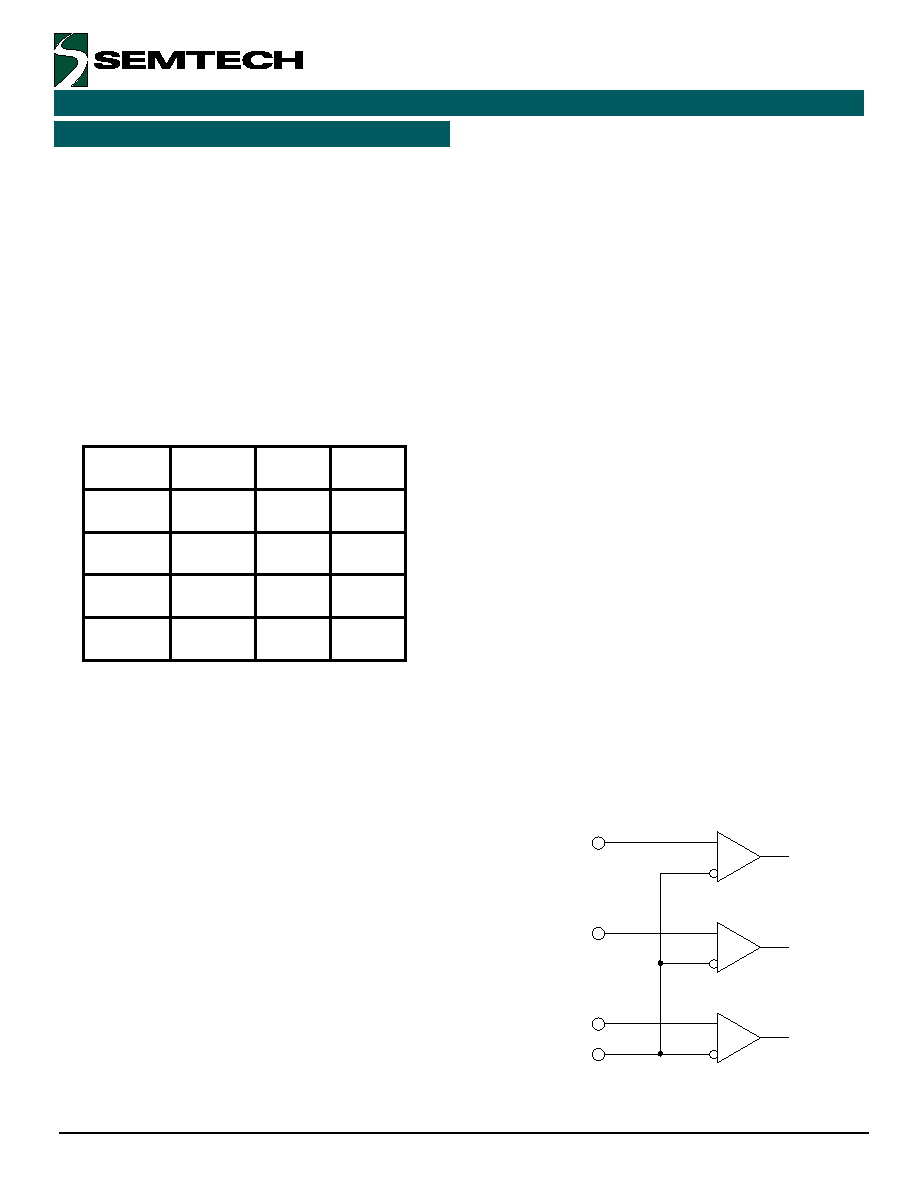
Figure 1. Digital Input Translation Stage
*
N
E
R
V
DN
E
T
VA
T
A
DT
U
O
D
10
X
Z
i
H
11
X
T
V
0X
0
L
V
0X
1
H
V
DATA
DVR EN*
VTT EN
VBB
相关PDF资料 |
PDF描述 |
|---|---|
| E86MON | E86MON - E86MON Software User's Manual |
| E88C312 | Microcontroller |
| E88C411-25 | DRAM/Cache Controller |
| E88C411-33 | DRAM/Cache Controller |
| E88C412 | System Controller |
相关代理商/技术参数 |
参数描述 |
|---|---|
| E84709-000 | 制造商:TE Connectivity 功能描述:SURGE PROTECTOR 200V BREAKOVER |
| E84784-000 | 制造商:TE Connectivity 功能描述:E84784-000 - Bulk 制造商:TE Connectivity 功能描述:TX40AB00-2208H |
| E84785-000 | 制造商:TE Connectivity 功能描述:DWP-125-3/16-0-150MM - Bulk |
| E84837-000 | 制造商:TE Connectivity 功能描述:VARISTOR 330V 20MM STRAIGHT LEAD 制造商:TE Connectivity 功能描述:VARISTOR 330V 10KA DISC 20MM |
| E848784 | 制造商:Elo Touch Solutions Inc 功能描述:15B1 TOUCHCOMPUTER - 15-INCH LCD, APR (ACOUSTIC PULSE RECOGN - Bulk |
发布紧急采购,3分钟左右您将得到回复。