- 您现在的位置:买卖IC网 > PDF目录11153 > EFM32TG842F8 (Energy Micro)IC MCU 32BIT 8KB FLASH LQFP64 PDF资料下载
参数资料
| 型号: | EFM32TG842F8 |
| 厂商: | Energy Micro |
| 文件页数: | 46/68页 |
| 文件大小: | 0K |
| 描述: | IC MCU 32BIT 8KB FLASH LQFP64 |
| 标准包装: | 1,000 |
| 系列: | Tiny Gecko |
| 核心处理器: | ARM? Cortex?-M3 |
| 芯体尺寸: | 32-位 |
| 速度: | 32MHz |
| 连通性: | I²C,IrDA,智能卡,SPI,UART/USART |
| 外围设备: | 欠压检测/复位,DMA,I²S,LCD,POR,PWM,WDT |
| 输入/输出数: | 53 |
| 程序存储器容量: | 8KB(8K x 8) |
| 程序存储器类型: | 闪存 |
| RAM 容量: | 2K x 8 |
| 电压 - 电源 (Vcc/Vdd): | 1.8 V ~ 3.8 V |
| 数据转换器: | A/D 8x12b,D/A 1x12b |
| 振荡器型: | 外部 |
| 工作温度: | -40°C ~ 85°C |
| 封装/外壳: | 64-TQFP |
| 包装: | 带卷 (TR) |
第1页第2页第3页第4页第5页第6页第7页第8页第9页第10页第11页第12页第13页第14页第15页第16页第17页第18页第19页第20页第21页第22页第23页第24页第25页第26页第27页第28页第29页第30页第31页第32页第33页第34页第35页第36页第37页第38页第39页第40页第41页第42页第43页第44页第45页当前第46页第47页第48页第49页第50页第51页第52页第53页第54页第55页第56页第57页第58页第59页第60页第61页第62页第63页第64页第65页第66页第67页第68页
...the world's most energy friendly microcontrollers
2013-06-28 - EFM32TG842FXX - d0072_Rev1.10
50
www.energymicro.com
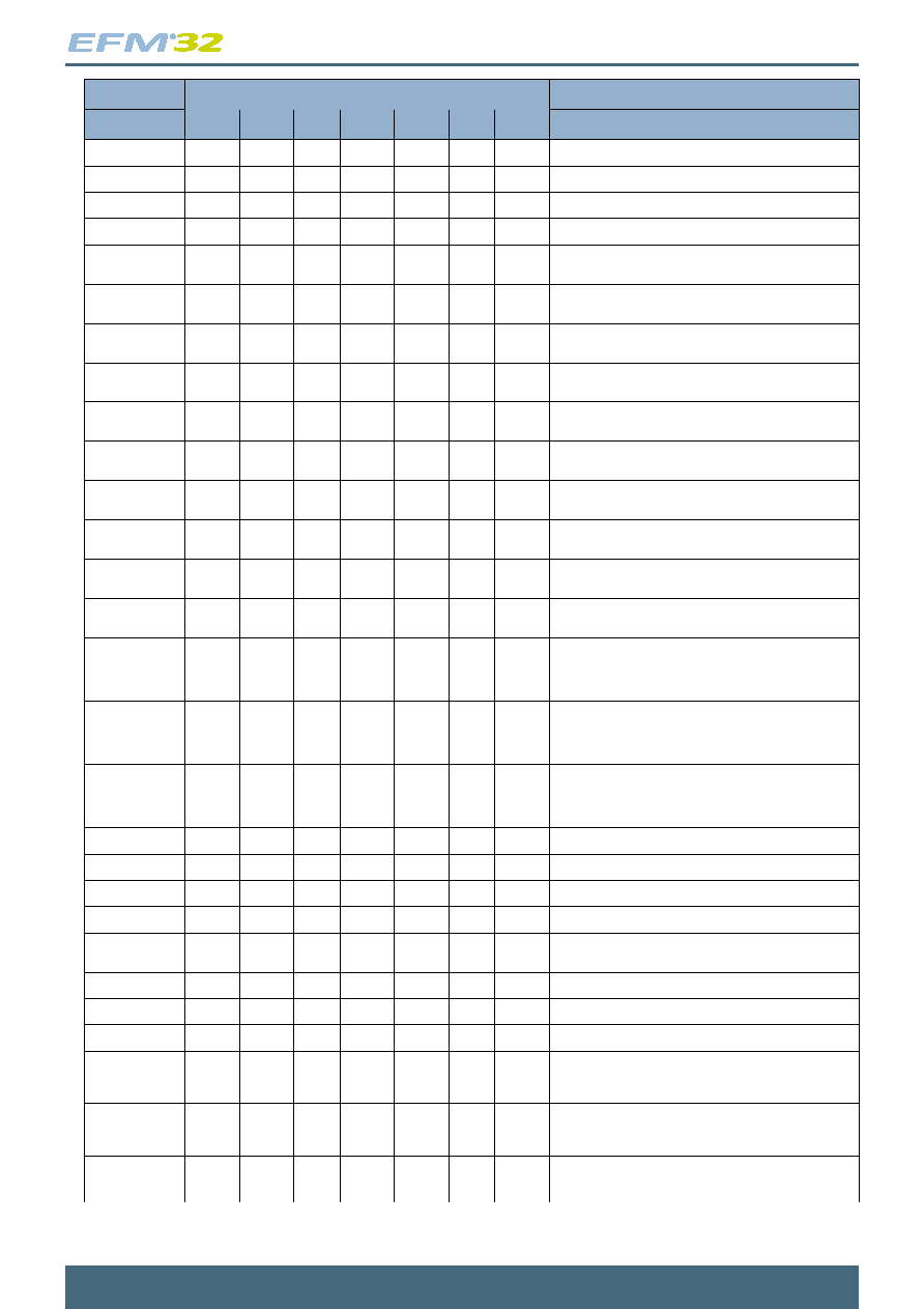
Alternate
LOCATION
Functionality
0
1
2
3
4
5
6
Description
BOOT_RX
PE11
Bootloader RX
BOOT_TX
PE10
Bootloader TX
CMU_CLK0
PA2
PC12
PD7
Clock Management Unit, clock output number 0.
CMU_CLK1
PA1
PD8
PE12
Clock Management Unit, clock output number 1.
DAC0_N0 /
OPAMP_N0
PC5
Operational Amplifier 0 external negative input.
DAC0_N1 /
OPAMP_N1
PD7
Operational Amplifier 1 external negative input.
DAC0_N2 /
OPAMP_N2
PD3
Operational Amplifier 2 external negative input.
DAC0_OUT0 /
OPAMP_OUT0
PB11
Digital to Analog Converter DAC0_OUT0 /
OPAMP output channel number 0.
DAC0_OUT0ALT /
OPAMP_OUT0ALT
PD0
Digital to Analog Converter DAC0_OUT0ALT /
OPAMP alternative output for channel 0.
DAC0_OUT1ALT /
OPAMP_OUT1ALT
PC12
PC13
PC14
PC15
PD1
Digital to Analog Converter DAC0_OUT1ALT /
OPAMP alternative output for channel 1.
DAC0_OUT2 /
OPAMP_OUT2
PD5
PD0
Digital to Analog Converter DAC0_OUT2 /
OPAMP output channel number 2.
DAC0_P0 /
OPAMP_P0
PC4
Operational Amplifier 0 external positive input.
DAC0_P1 /
OPAMP_P1
PD6
Operational Amplifier 1 external positive input.
DAC0_P2 /
OPAMP_P2
PD4
Operational Amplifier 2 external positive input.
DBG_SWCLK
PF0
Debug-interface Serial Wire clock input.
Note that this function is enabled to pin out of reset, and has
a built-in pull down.
DBG_SWDIO
PF1
Debug-interface Serial Wire data input / output.
Note that this function is enabled to pin out of reset, and has
a built-in pull up.
DBG_SWO
PF2
PC15
Debug-interface Serial Wire viewer Output.
Note that this function is not enabled after reset, and must be
enabled by software to be used.
GPIO_EM4WU0
PA0
Pin can be used to wake the system up from EM4
GPIO_EM4WU3
PF1
Pin can be used to wake the system up from EM4
GPIO_EM4WU4
PF2
Pin can be used to wake the system up from EM4
GPIO_EM4WU5
PE13
Pin can be used to wake the system up from EM4
HFXTAL_N
PB14
High Frequency Crystal negative pin. Also used as external
optional clock input pin.
HFXTAL_P
PB13
High Frequency Crystal positive pin.
I2C0_SCL
PA1
PD7
PC7
PF1
PE13
I2C0 Serial Clock Line input / output.
I2C0_SDA
PA0
PD6
PC6
PF0
PE12
I2C0 Serial Data input / output.
LCD_BCAP_N
PA13
LCD voltage booster (optional), boost capacitor, negative pin.
If using the LCD voltage booster, connect a 22 nF capacitor
between LCD_BCAP_N and LCD_BCAP_P.
LCD_BCAP_P
PA12
LCD voltage booster (optional), boost capacitor, positive pin.
If using the LCD voltage booster, connect a 22 nF capacitor
between LCD_BCAP_N and LCD_BCAP_P.
LCD_BEXT
PA14
LCD voltage booster (optional), boost output. If using the
LCD voltage booster, connect a 1 uF capacitor between this
pin and VSS.
相关PDF资料 |
PDF描述 |
|---|---|
| VI-B6B-IX-F1 | CONVERTER MOD DC/DC 95V 75W |
| EFM32TG840F8 | MCU 32BIT 8KB FLASH 64-QFN |
| EFM32G200F32 | MCU 32BIT 32KB FLASH 32-QFN |
| C8051F562-IM | IC 8051 MCU 32K FLASH 32-QFN |
| VI-B6B-IW-F4 | CONVERTER MOD DC/DC 95V 100W |
相关代理商/技术参数 |
参数描述 |
|---|---|
| EFM32TG842F8-QFP64 | 制造商:Energy Micro AS 功能描述:TINY GECKO MCU - Tape and Reel 制造商:Energy Micro AS 功能描述:IC MCU 32BIT 8KB FLASH 64TQFP |
| EFM32TG842F8-QFP64T | 制造商:Energy Micro AS 功能描述:32 BIT ARM MPU, TINY GECKO - Trays |
| EFM32TG842F8-QFP64-T | 制造商:Energy Micro AS 功能描述:IC MCU 32BIT 8KB FLASH 64TQFP |
| EFM32TG842F8-T | 制造商:Energy Micro AS 功能描述:IC MCU 32BIT 8KB FLASH 64TQFP |
| EFM32-TG-STK3300 | 功能描述:开发板和工具包 - ARM TG Starter Kit RoHS:否 制造商:Arduino 产品:Development Boards 工具用于评估:ATSAM3X8EA-AU 核心:ARM Cortex M3 接口类型:DAC, ICSP, JTAG, UART, USB 工作电源电压:3.3 V |
发布紧急采购,3分钟左右您将得到回复。