- 您现在的位置:买卖IC网 > PDF目录17091 > EK-V6-ML631-G (Xilinx Inc)VIRTEX-6 HXT FPGA ML631 EVAL KIT PDF资料下载
参数资料
| 型号: | EK-V6-ML631-G |
| 厂商: | Xilinx Inc |
| 文件页数: | 51/65页 |
| 文件大小: | 0K |
| 描述: | VIRTEX-6 HXT FPGA ML631 EVAL KIT |
| 标准包装: | 1 |
| 系列: | Virtex® 6 HXT |
| 类型: | FPGA |
| 适用于相关产品: | Virtex?-6 XC6VHX565T |
| 所含物品: | 板,线缆,软件和文档 |
第1页第2页第3页第4页第5页第6页第7页第8页第9页第10页第11页第12页第13页第14页第15页第16页第17页第18页第19页第20页第21页第22页第23页第24页第25页第26页第27页第28页第29页第30页第31页第32页第33页第34页第35页第36页第37页第38页第39页第40页第41页第42页第43页第44页第45页第46页第47页第48页第49页第50页当前第51页第52页第53页第54页第55页第56页第57页第58页第59页第60页第61页第62页第63页第64页第65页
�� �
�
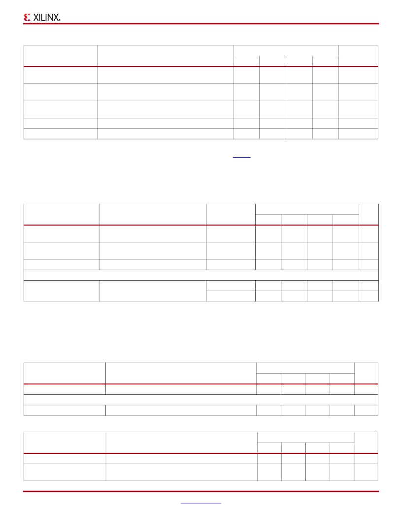
�Virtex-6� FPGA� Data� Sheet:� DC� and� Switching� Characteristics�
�Table� 59:� Configuration� Switching� Characteristics� (Cont’d)�
�Symbol�
�Description�
�-3�
�Speed� Grade�
�-2� -1�
�-1L�
�Units�
�T� MMCMDCK_DI� /�
�T� MMCMCKD_DI�
�T� MMCMDCK_DEN� /�
�T� MMCMCKD_DEN�
�T� MMCMDCK_DWE� /�
�T� MMCMCKD_DWE�
�T� MMCMCKO_DO�
�T� MMCMCKO_DRDY�
�DI� Setup/Hold�
�DEN� Setup/Hold� time�
�DWE� Setup/Hold� time�
�CLK� to� out� of� DO� (3)�
�CLK� to� out� of� DRDY�
�1.25/�
�0.00�
�1.25/�
�0.00�
�1.25/�
�0.00�
�2.60�
�0.32�
�1.40/�
�0.00�
�1.40/�
�0.00�
�1.40/�
�0.00�
�3.02�
�0.34�
�1.63/�
�0.00�
�1.63/�
�0.00�
�1.63/�
�0.00�
�3.64�
�0.38�
�1.64/�
�0.00�
�1.64/�
�0.00�
�1.64/�
�0.00�
�3.68�
�0.38�
�ns�
�ns�
�ns�
�ns�
�ns�
�Notes:�
�1.�
�2.�
�3.�
�To� support� longer� delays� in� configuration,� use� the� design� solutions� described� in� UG360� :� Virtex-6� FPGA� Configuration� User� Guide� .�
�Only� during� configuration,� the� last� edge� is� determined� by� a� weak� pull-up/pull-down� resistor� in� the� I/O.�
�DO� will� hold� until� next� DRP� operation.�
�Clock� Buffers� and� Networks�
�Table� 60:� Global� Clock� Switching� Characteristics� (Including� BUFGCTRL)�
�Symbol�
�Description�
�Devices�
�-3�
�Speed� Grade�
�-2� -1�
�-1L�
�Units�
�T� BCCCK_CE� /T� BCCKC_CE� (1)�
�T� BCCCK_S� /T� BCCKC_S� (1)�
�T� BCCKO_O� (2)�
�CE� pins� Setup/Hold�
�S� pins� Setup/Hold�
�BUFGCTRL� delay� from� I0/I1� to� O�
�All�
�All�
�All�
�0.11/�
�0.00�
�0.11/�
�0.00�
�0.07�
�0.13/�
�0.00�
�0.13/�
�0.00�
�0.08�
�0.16/�
�0.00�
�0.16/�
�0.00�
�0.10�
�0.13/�
�0.00�
�0.13/�
�0.00�
�0.10�
�ns�
�ns�
�ns�
�Maximum� Frequency�
�F� MAX�
�Global� clock� tree� (BUFG)�
�All� except� LX760�
�LX760�
�800�
�N/A�
�750�
�700�
�700�
�700�
�667�
�667�
�MHz�
�MHz�
�Notes:�
�1.�
�2.�
�T� BCCCK_CE� and� T� BCCKC_CE� must� be� satisfied� to� assure� glitch-free� operation� of� the� global� clock� when� switching� between� clocks.� These�
�parameters� do� not� apply� to� the� BUFGMUX_VIRTEX4� primitive� that� assures� glitch-free� operation.� The� other� global� clock� setup� and� hold�
�times� are� optional;� only� needing� to� be� satisfied� if� device� operation� requires� simulation� matches� on� a� cycle-for-cycle� basis� when� switching�
�between� clocks.�
�T� BGCKO_O� (BUFG� delay� from� I0� to� O)� values� are� the� same� as� T� BCCKO_O� values.�
�Table� 61:� Input/Output� Clock� Switching� Characteristics� (BUFIO)�
�Symbol�
�Description�
�-3�
�Speed� Grade�
�-2� -1�
�-1L�
�Units�
�T� BIOCKO_O�
�Clock� to� out� delay� from� I� to� O�
�0.14�
�0.16�
�0.18�
�0.21�
�ns�
�Maximum� Frequency�
�F� MAX�
�I/O� clock� tree� (BUFIO)�
�800�
�800�
�710�
�710�
�MHz�
�Table� 62:� Regional� Clock� Switching� Characteristics� (BUFR)�
�Symbol�
�Description�
�-3�
�Speed� Grade�
�-2� -1�
�-1L�
�Units�
�T� BRCKO_O�
�T� BRCKO_O_BYP�
�Clock� to� out� delay� from� I� to� O�
�Clock� to� out� delay� from� I� to� O� with� Divide� Bypass� attribute�
�set�
�0.56�
�0.28�
�0.62�
�0.31�
�0.73�
�0.36�
�0.82�
�0.41�
�ns�
�ns�
�DS152� (v3.6)� March� 18,� 2014�
�Product� Specification�
��51�
�相关PDF资料 |
PDF描述 |
|---|---|
| EK-V6-ML630-G | VIRTEX-6 HXT FPGA ML630 EVAL KIT |
| ECM18DRKN-S13 | CONN EDGECARD 36POS .156 EXTEND |
| EK-V6-ML630-G-J | VIRTEX-6 HXT FPGA ML630 EVAL KIT |
| C8051F020-TB | BOARD PROTOTYPING W/C8051F020 |
| SDR-T2 | SCOTCH CODE REFILL T2 |
相关代理商/技术参数 |
参数描述 |
|---|---|
| EK-V6-ML631-G-J | 功能描述:VIRTEX-6 HXT FPGA ML631 EVAL KIT RoHS:是 类别:编程器,开发系统 >> 通用嵌入式开发板和套件(MCU、DSP、FPGA、CPLD等) 系列:Virtex® 6 HXT 标准包装:1 系列:PICDEM™ 类型:MCU 适用于相关产品:PIC10F206,PIC16F690,PIC16F819 所含物品:板,线缆,元件,CD,PICkit 编程器 产品目录页面:659 (CN2011-ZH PDF) |
| EK-V7-VC707-CES-G | 功能描述:VIRTEX-7 VC707 EVAL KIT RoHS:是 类别:编程器,开发系统 >> 通用嵌入式开发板和套件(MCU、DSP、FPGA、CPLD等) 系列:Virtex®-7 标准包装:1 系列:PICDEM™ 类型:MCU 适用于相关产品:PIC10F206,PIC16F690,PIC16F819 所含物品:板,线缆,元件,CD,PICkit 编程器 产品目录页面:659 (CN2011-ZH PDF) |
| EK-V7-VC707-CES-G-J | 功能描述:VIRTEX-7 VC707 EVAL KIT JAPAN RoHS:是 类别:编程器,开发系统 >> 通用嵌入式开发板和套件(MCU、DSP、FPGA、CPLD等) 系列:Virtex®-7 标准包装:1 系列:PICDEM™ 类型:MCU 适用于相关产品:PIC10F206,PIC16F690,PIC16F819 所含物品:板,线缆,元件,CD,PICkit 编程器 产品目录页面:659 (CN2011-ZH PDF) |
| EK-V7-VC707-G | 制造商:Xilinx 功能描述:VIRTEX-7 FPGA VC707 EVALUATION KIT - Boxed Product (Development Kits) 制造商:Xilinx 功能描述:KIT EVAL VIRTEX7 VC707 制造商:Xilinx 功能描述:VIRTEX-7 VC707 FPGA EVAL KIT |
| EK-V7-VC707-G-J | 制造商:Xilinx 功能描述:KIT EVAL VIRTEX7 VC707 JAPAN |
发布紧急采购,3分钟左右您将得到回复。