- 您现在的位置:买卖IC网 > PDF目录97899 > EL2120CN 100 MHz Current Feedback Amplifier PDF资料下载
参数资料
| 型号: | EL2120CN |
| 元件分类: | 运算放大器 |
| 英文描述: | 100 MHz Current Feedback Amplifier |
| 中文描述: | 100 MHz电流反馈放大器 |
| 文件页数: | 5/12页 |
| 文件大小: | 354K |
| 代理商: | EL2120CN |
EL2120C
100 MHz Current Feedback Amplifier
Absolute Maximum Ratings (T
A
e
25 C)
Voltage between Va and Vb
33V
Voltage at aIN
b
IN VOUT
(Vb) b 05V to (Va) a 05V
Voltage between
a
IN and b IN
g
5V
Voltage at Disable
(Va) b 10V to (Va) a 05V
Current into aIN
b
IN and Disable
g
5mA
Output Current
g
50 mA
Internal Power Dissipation
See Curves
Operating Ambient
Temperature Range
0 to 75 C
Operating Junction Temperature
P-DIP or SO
150 C
Storage Temperature Range
b
65 Cto a150 C
Important Note
All parameters having MinMax specifications are guaranteed The Test Level column indicates the specific device testing actually
performed during production and Quality inspection Elantec performs most electrical tests using modern high-speed automatic test
equipment specifically the LTX77 Series system Unless otherwise noted all tests are pulsed tests therefore TJeTCeTA
Test Level
Test Procedure
I
100% production tested and QA sample tested per QA test plan QCX0002
II
100% production tested at TA e 25 C and QA sample tested at TA e 25 C
TMAX and TMIN per QA test plan QCX0002
III
QA sample tested per QA test plan QCX0002
IV
Parameter is guaranteed (but not tested) by Design and Characterization Data
V
Parameter is typical value at TA e 25 C for information purposes only
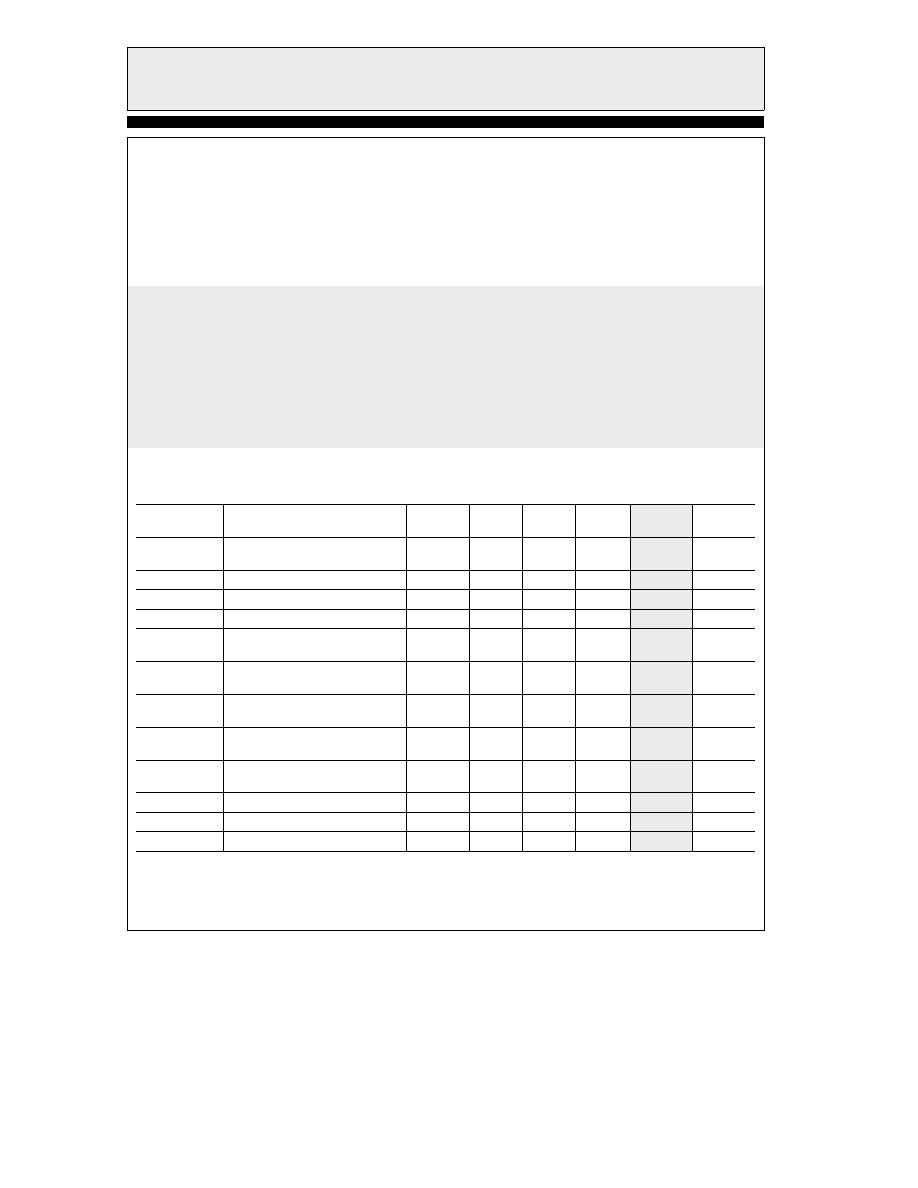
Open Loop DC Electrical Characteristics
VS e g5V RL e 150X TA e 25 C unless otherwise specified
Parameter
Description
Temp
Min
Typ
Max
Test
Units
Level
VOS
Input Offset Voltage
Full
4
20
II
mV
VS e g15V
Full
2
25
II
mV
DVOS DT
Input Offset Drift
Full
20
V
mV C
IBa
a
VIN Input Bias Current
Full
5
15
II
mA
IBb
b
VIN Input Bias Current
Full
10
50
II
mA
CMRR
Common-Mode Rejection
Full
50
55
II
dB
(Note 1)
b
ICMR
b
Input Current Common-Mode
Full
8
20
II
mAV
Rejection (Note 1)
PSRR
Power Supply Rejection
Full
65
80
II
dB
(Note 2)
a
IPSR
a
Input Current Power Supply
25 C
003
V
mAV
Rejection (Note 2)
b
IPSR
b
Input Current Power Supply
Full
06
5
II
mAV
Rejection (Note 2)
ROL
Transimpedance
Full
70
140
II
k
X
AVOL
Voltage Gain
Full
58
66
II
dB
a
RIN
a
VIN Input Impedance
25 C2
V
M
X
2
TD
is
32in
相关PDF资料 |
PDF描述 |
|---|---|
| EL2120CS | 100 MHz Current Feedback Amplifier |
| EL2126CN | Ultra-low Noise, Low Power, Wideband Amplifier |
| EL2126CS | Ultra-low Noise, Low Power, Wideband Amplifier |
| EL2126CW | Ultra-low Noise, Low Power, Wideband Amplifier |
| EL2126C | Ultra-low Noise, Low Power, Wideband Amplifier |
相关代理商/技术参数 |
参数描述 |
|---|---|
| EL2120CS | 制造商:INTERSIL 制造商全称:Intersil Corporation 功能描述:100MHz Current Feedback Amplifier |
| EL2125 | 制造商:INTERSIL 制造商全称:Intersil Corporation 功能描述:Ultra-Low Noise, Low Power, Wideband Amplifier |
| EL2125 WAF | 制造商:Intersil Corporation 功能描述: |
| EL2125_07 | 制造商:INTERSIL 制造商全称:Intersil Corporation 功能描述:Ultra-Low Noise, Low Power, Wideband Amplifier |
| EL2125C | 制造商:ELANTEC 制造商全称:ELANTEC 功能描述:Ultra-low Noise, Low Power, Wideband Amplifier |
发布紧急采购,3分钟左右您将得到回复。