参数资料
| 型号: | EL2125CS |
| 厂商: | Intersil |
| 文件页数: | 6/16页 |
| 文件大小: | 0K |
| 描述: | IC AMP WIDEBAND LP LN 8-SOIC |
| 标准包装: | 97 |
| 放大器类型: | 电压反馈 |
| 电路数: | 1 |
| 转换速率: | 185 V/µs |
| -3db带宽: | 220MHz |
| 电流 - 输入偏压: | 22µA |
| 电压 - 输入偏移: | 600µV |
| 电流 - 电源: | 10.8mA |
| 电流 - 输出 / 通道: | 250mA |
| 电压 - 电源,单路/双路(±): | 5 V ~ 30 V,±2.5 V ~ 15 V |
| 工作温度: | -45°C ~ 85°C |
| 安装类型: | 表面贴装 |
| 封装/外壳: | 8-SOIC(0.154",3.90mm 宽) |
| 供应商设备封装: | 8-SOIC |
| 包装: | 管件 |
14
FN7045.3
May 4, 2007
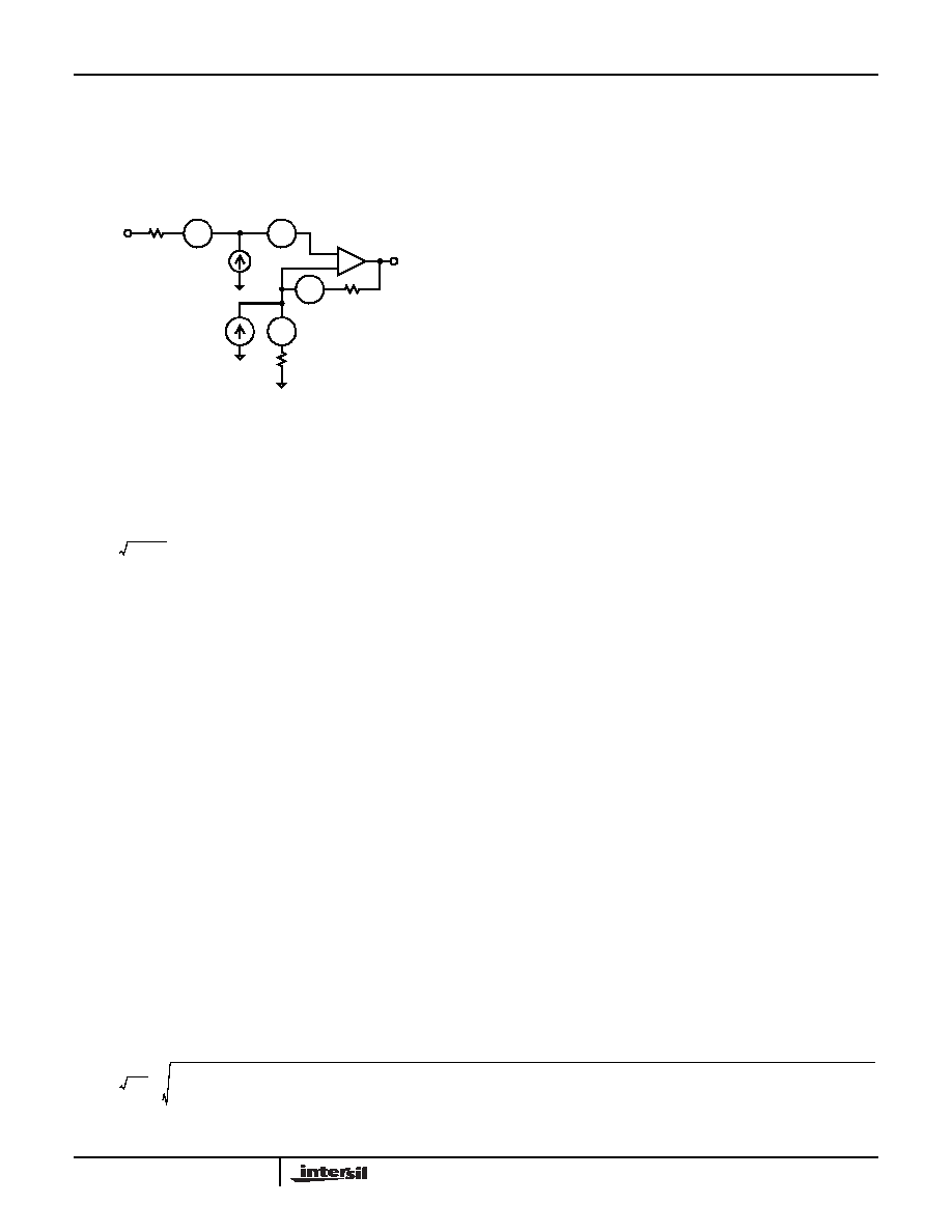
Noise Calculations
The primary application for the EL2125 is to amplify very
small signals. To maintain the proper signal-to-noise ratio, it
is essential to minimize noise contribution from the amplifier.
Figure 51 below shows all the noise sources for all the
components around the amplifier.
FIGURE 51.
VN is the amplifier input voltage noise
IN+ is the amplifier positive input current noise
IN- is the amplifier negative input current noise
VRX is the thermal noise associated with each resistor:
where:
k is Boltzmann's constant = 1.380658 x 10⁻²³
T is temperature in degrees Kelvin (273+ °C)
The total noise due to the amplifier seen at the output of the
amplifier can be calculated by using the equation below
(Figure 52).
As the equation shows, to keep noise at a minimum, small
resistor values should be used. At higher amplifier gain
configuration where R2 is reduced, the noise due to IN-, R2,
and R1 decreases and the noise caused by IN+, VN, and R3
starts to dominate. Because noise is summed in a root-mean-
squares method, noise sources smaller than 25% of the largest
noise source can be ignored. This can greatly simplify the
formula and make noise calculation much easier to calculate.
Output Drive Capability
The EL2125 is designed to drive low impedance load. It can
easily drive 6VP-P signal into a 100Ω load. This high output
drive capability makes the EL2125 an ideal choice for RF, IF,
and video applications. Furthermore, the EL2125 is current-
limited at the output, allowing it to withstand momentary short to
ground. However, the power dissipation with output-shorted
cannot exceed the power dissipation capability of the package.
Driving Cables and Capacitive Loads
Although the EL2125 is designed to drive low impedance
load, capacitive loads will decrease the amplifier's phase
margin. As shown the in the performance curves, capacitive
load can result in peaking, overshoot and possible
oscillation. For optimum AC performance, capacitive loads
should be reduced as much as possible or isolated with a
series resistor between 5
Ω to 20Ω. When driving coaxial
cables, double termination is always recommended for
reflection-free performance. When properly terminated, the
capacitance of the coaxial cable will not add to the capacitive
load seen by the amplifier.
Power Supply Bypassing And Printed Circuit
Board Layout
As with any high frequency devices, good printed circuit
board layout is essential for optimum performance. Ground
plane construction is highly recommended. Lead lengths
should be kept as short as possible. The power supply pins
must be closely bypassed to reduce the risk of oscillation.
The combination of a 4.7F tantalum capacitor in parallel
with 0.1F ceramic capacitor has been proven to work well
when placed at each supply pin. For single supply operation,
where pin 4 (VS-) is connected to the ground plane, a single
4.7F tantalum capacitor in parallel with a 0.1F ceramic
capacitor across pins 7 (VS+) and pin 4 (VS-) will suffice.
For good AC performance, parasitic capacitance should be
kept to a minimum. Ground plane construction again should
be used. Small chip resistors are recommended to minimize
series inductance. Use of sockets should be avoided since
they add parasitic inductance and capacitance which will
result in additional peaking and overshoot.
Supply Voltage Range and Single Supply
Operation
The EL2125 has been designed to operate with supply
voltage range of ±2.5V to ±15V. With a single supply, the
EL2125 will operate from +5V to +30V. Pins 4 and 7 are the
power supply pins. The positive power supply is connected
to pin 7. When used in single supply mode, pin 4 is
connected to ground. When used in dual supply mode, the
negative power supply is connected to pin 4.
As the power supply voltage decreases from +30V to +5V, it
becomes necessary to pay special attention to the input
voltage range. The EL2125 has an input voltage range of
0.4V from the negative supply to 1.2V from the positive
supply. So, for example, on a single +5V supply, the EL2125
has an input voltage range which spans from 0.4V to 3.8V.
The output range of the EL2125 is also quite large, on a +5V
supply, it swings from 0.4V to 3.6V.
-
+
VON
VIN
IN+
IN-
R2
R3
R1
VN
VR3
VR2
VR1
VRX
4kTRx
=
VON
BW
=
VN
2
1
R1
R2
-------
+
2
×
IN-
2
R1
2
IN+
2
R3
2
1
R1
R2
-------
+
2
×
+
×
4KTR1 4KTR2
R1
R2
-------
2
×
+
×
4K T R3 1
R1
R2
-------
+
2
×
++
+
×
FIGURE 52.
EL2125
相关PDF资料 |
PDF描述 |
|---|---|
| TA35-CFTWF050C0 | CIRC BREAKER/WHITE ROCKER SP 5A |
| PGD009S030BSR01 | SUPPRESSOR ESD 9 PIN D SUB REAR |
| EL2045CN | IC OP AMP 100MHZ HS 8-PDIP |
| 953426-6602-AR | CONN SOCKET 26POS 2MM VERT T/H |
| CA3140M | IC OP AMP BIMOS 4.5MHZ 8-SOIC |
相关代理商/技术参数 |
参数描述 |
|---|---|
| EL2125CS-T13 | 功能描述:IC AMP ULT LO NOISE/POWER 8-SOIC RoHS:否 类别:集成电路 (IC) >> Linear - Amplifiers - Instrumentation 系列:- 标准包装:1 系列:- 放大器类型:通用 电路数:4 输出类型:满摆幅 转换速率:0.6 V/µs 增益带宽积:1MHz -3db带宽:- 电流 - 输入偏压:2pA 电压 - 输入偏移:1000µV 电流 - 电源:85µA 电流 - 输出 / 通道:20mA 电压 - 电源,单路/双路(±):1.8 V ~ 6 V 工作温度:-40°C ~ 125°C 安装类型:表面贴装 封装/外壳:14-SOIC(0.154",3.90mm 宽) 供应商设备封装:14-SOICN 包装:剪切带 (CT) 产品目录页面:680 (CN2011-ZH PDF) 其它名称:MCP6L04T-E/SLCT |
| EL2125CS-T7 | 功能描述:IC AMP ULT LO NOISE/POWER 8-SOIC RoHS:否 类别:集成电路 (IC) >> Linear - Amplifiers - Instrumentation 系列:- 标准包装:1 系列:- 放大器类型:通用 电路数:4 输出类型:满摆幅 转换速率:0.6 V/µs 增益带宽积:1MHz -3db带宽:- 电流 - 输入偏压:2pA 电压 - 输入偏移:1000µV 电流 - 电源:85µA 电流 - 输出 / 通道:20mA 电压 - 电源,单路/双路(±):1.8 V ~ 6 V 工作温度:-40°C ~ 125°C 安装类型:表面贴装 封装/外壳:14-SOIC(0.154",3.90mm 宽) 供应商设备封装:14-SOICN 包装:剪切带 (CT) 产品目录页面:680 (CN2011-ZH PDF) 其它名称:MCP6L04T-E/SLCT |
| EL2125CSZ | 功能描述:运算放大器 - 运放 EL2125CSZ LW NOISE REC A=10 RoHS:否 制造商:STMicroelectronics 通道数量:4 共模抑制比(最小值):63 dB 输入补偿电压:1 mV 输入偏流(最大值):10 pA 工作电源电压:2.7 V to 5.5 V 安装风格:SMD/SMT 封装 / 箱体:QFN-16 转换速度:0.89 V/us 关闭:No 输出电流:55 mA 最大工作温度:+ 125 C 封装:Reel |
| EL2125CSZ-T13 | 功能描述:高速运算放大器 EL2125CSZ LW NOISE CVR A=10 RoHS:否 制造商:Texas Instruments 通道数量:1 电压增益 dB:116 dB 输入补偿电压:0.5 mV 转换速度:55 V/us 工作电源电压:36 V 电源电流:7.5 mA 最大工作温度:+ 85 C 安装风格:SMD/SMT 封装 / 箱体:SOIC-8 封装:Tube |
| EL2125CSZ-T7 | 功能描述:高速运算放大器 EL2125CSZ LW NOISE CVR A=11 RoHS:否 制造商:Texas Instruments 通道数量:1 电压增益 dB:116 dB 输入补偿电压:0.5 mV 转换速度:55 V/us 工作电源电压:36 V 电源电流:7.5 mA 最大工作温度:+ 85 C 安装风格:SMD/SMT 封装 / 箱体:SOIC-8 封装:Tube |
发布紧急采购,3分钟左右您将得到回复。