- 您现在的位置:买卖IC网 > PDF目录97899 > EL2140 150 MHz Differential Twisted Pair Driver PDF资料下载
参数资料
| 型号: | EL2140 |
| 英文描述: | 150 MHz Differential Twisted Pair Driver |
| 中文描述: | 150 MHz的差分双绞线驱动器 |
| 文件页数: | 5/12页 |
| 文件大小: | 219K |
| 代理商: | EL2140 |
EL2140C2141C
150 MHz Differential Twisted Pair Driver
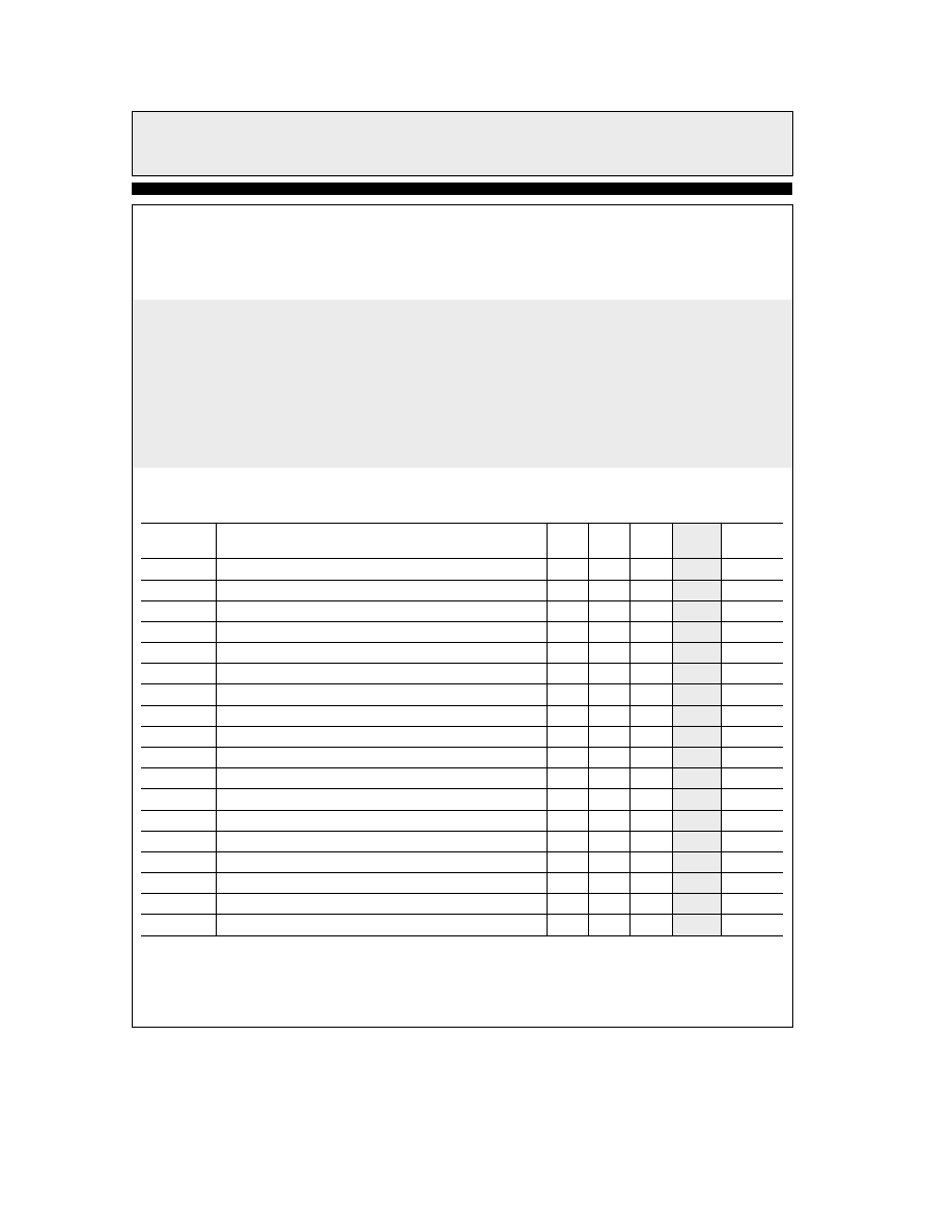
Absolute Maximum Ratings
Supply Voltage (VCC–VEE)
0V – 126V
Maximum Output Current
g
60 mA
Storage Temperature Range
b
65 Cto a150 C
Operating Junction Temperaure
a
150 C
Recommended Operating Temperature
b
40 Cto85 C
VIN VINB VREF
VEEa08V (MIN) to VCCb08V (MAX)
VIN–VINB
g
5V
Important Note
All parameters having MinMax specifications are guaranteed The Test Level column indicates the specific device testing actually
performed during production and Quality inspection Elantec performs most electrical tests using modern high-speed automatic test
equipment specifically the LTX77 Series system Unless otherwise noted all tests are pulsed tests therefore TJeTCeTA
Test Level
Test Procedure
I
100% production tested and QA sample tested per QA test plan QCX0002
II
100% production tested at TA e 25 C and QA sample tested at TA e 25 C
TMAX and TMIN per QA test plan QCX0002
III
QA sample tested per QA test plan QCX0002
IV
Parameter is guaranteed (but not tested) by Design and Characterization Data
V
Parameter is typical value at TA e 25 C for information purposes only
DC Electrical Characteristics
VCC ea5V VEE eb5V TA e 25 C VIN e 0V RL e 200 unless otherwise specified
Parameter
Description
Min
Typ
Max
Test
Units
Level
Vsupply
Supply Operating Range (VCC–VEE)
g
30
g
50
g
63
I
V
IS
Power Supply Current (No Load)
11
14
I
mA
VOS
Input Referred Offset Voltage
b
25
10
40
I
mV
IIN
Input Bias Current (VIN VINB VREF)
b
20
6
20
I
mA
ZIN
Differential Input Impedance
400
V
k
X
VDIFF
Differential Input Range
g
20
g
23
I
V
AV
Voltage Gain (EL2140C) VIN e 2V pk-pk
195
1985
202
I
VV
AVOL
Open Loop Voltage Gain (EL2141C)
75
V
dB
VCM
Input Common Mode Voltage Range (EL2140C)
b
26
a
40
I
V
VOUT(200)
Output Voltage Swing (200
X load VOUT to VOUTB) (EL2141C)
g
34
g
36
I
V
VOUT(100)
Output Voltage Swing (100
X Load VOUT to VOUTB) (EL2141C)
g
29
g
31
I
V
VN
Input Referred Voltage Noise
36
V
nV SHz
VREF
Output Voltage Control Range (EL2140C)
b
25
a
33
I
V
VREFOS
Output Offset Relative to VREF
b
60
b
25
a
60
I
mV
PSRR
Power Supply Rejection Ratio
60
70
I
dB
IOUT(min)
Minimum Output Current
50
60
I
mA
CMRR
Input Common Mode Rejection Ratio (EL2140C) VCM e g 2V
60
70
I
dB
ROUT
(VOUT e VOUTB e 0V) Output Impedence
01
V
X
2
TD
is
03in
TD
is
37in
相关PDF资料 |
PDF描述 |
|---|---|
| EL2140CN | 150 MHz Differential Twisted Pair Driver |
| EL2140CS | 150 MHz Differential Twisted Pair Driver |
| EL2141CN | 150 MHz Differential Twisted Pair Driver |
| EL2141CS | 150 MHz Differential Twisted Pair Driver |
| EL2141C | 150 MHz High Bandwidth Amplifier (Differential Twisted Pair Driver)(150 MHz宽带放大器(差分双绞线驱动器)) |
相关代理商/技术参数 |
参数描述 |
|---|---|
| EL2140C | 制造商:ELANTEC 制造商全称:ELANTEC 功能描述:150 MHz Differential Twisted Pair Driver |
| EL2140CN | 制造商:ELANTEC 制造商全称:ELANTEC 功能描述:150 MHz Differential Twisted Pair Driver |
| EL2140CS | 制造商:Rochester Electronics LLC 功能描述: 制造商:Intersil Corporation 功能描述: |
| EL2140CS-T13 | 制造商:Rochester Electronics LLC 功能描述: 制造商:Intersil Corporation 功能描述: |
| EL2141 | 制造商:INTERSIL 制造商全称:Intersil Corporation 功能描述:150MHz Differential Twisted Pair Driver |
发布紧急采购,3分钟左右您将得到回复。