参数资料
| 型号: | EL2227CY-T7 |
| 厂商: | Intersil |
| 文件页数: | 3/14页 |
| 文件大小: | 0K |
| 描述: | IC AMP DUAL LOW NOISE 8-MSOP |
| 标准包装: | 1,500 |
| 放大器类型: | 电压反馈 |
| 电路数: | 2 |
| 转换速率: | 50 V/µs |
| 增益带宽积: | 137MHz |
| -3db带宽: | 115MHz |
| 电流 - 输入偏压: | 3.4µA |
| 电压 - 输入偏移: | 200µV |
| 电流 - 电源: | 4.8mA |
| 电流 - 输出 / 通道: | 180mA |
| 电压 - 电源,单路/双路(±): | 5 V ~ 24 V,±2.5 V ~ 12 V |
| 工作温度: | -40°C ~ 85°C |
| 安装类型: | 表面贴装 |
| 封装/外壳: | 8-TSSOP,8-MSOP(0.118",3.00mm 宽) |
| 供应商设备封装: | 8-MSOP |
| 包装: | 带卷 (TR) |
11
FN7058.4
September 14 ,2010
Applications Information
Product Description
The EL2227 is a dual voltage feedback operational amplifier
designed especially for DMT ADSL and other applications
requiring very low voltage and current noise. It also features
low distortion while drawing moderately low supply current
and is built on Elantec's proprietary high-speed
complementary bipolar process. The EL2227 use a classical
voltage-feedback topology, which allows them to be used in
a variety of applications where current-feedback amplifiers
are not appropriate because of restrictions placed upon the
feedback element used with the amplifier. The conventional
topology of the EL2227 allows, for example, a capacitor to
be placed in the feedback path, making it an excellent choice
for applications such as active filters, sample-and-holds, or
integrators.
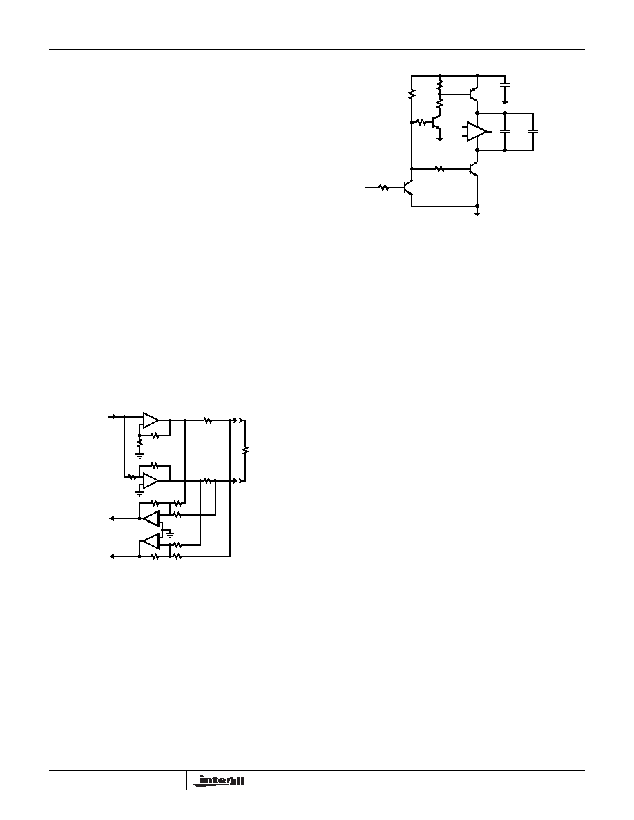
ADSL CPE Applications
The low noise EL2227 amplifier is specifically designed for
the dual differential receiver amplifier function with ADSL
transceiver hybrids, as well as other low-noise amplifier
applications. A typical ADSL CPE line interface circuit is
shown in Figure 38. The EL2227 is used in receiving DMT
down stream signal. With careful transceiver hybrid design
and the EL2227 1.9nV/
√Hz voltage noise and 1.2pA/√Hz
current noise performance, -140dBm/Hz system background
noise performance can be easily achieved.
Disable Function
The EL2227 is in the standard dual amplifier package without
the enable/disable function. A simple way to implement the
enable/disable function is depicted in Figure 39. When
disabled, both the positive and negative supply voltages are
disconnected (see Figure 39).
Power Dissipation
With the wide power supply range and large output drive
capability of the EL2227, it is possible to exceed the +150°C
maximum junction temperatures under certain load and power
supply conditions. It is therefore important to calculate the
maximum junction temperature (TJMAX) for all applications to
determine if power supply voltages, load conditions, or package
type need to be modified for the EL2227 to remain in the safe
operating area. These parameters are related in Equation 1:
where:
PDMAXTOTAL is the sum of the maximum power
dissipation of each amplifier in the package (PDMAX)
PDMAX for each amplifier can be calculated using
Equation 2:
where:
TMAX = Maximum Ambient Temperature
θJA = Thermal Resistance of the Package
PDMAX = Maximum Power Dissipation of 1 Amplifier
VS = Supply Voltage
IMAX = Maximum Supply Current of 1 Amplifier
VOUTMAX = Maximum Output Voltage Swing of the
Application
RL = Load Resistance
To serve as a guide for the user, we can calculate maximum
allowable supply voltages for the example of the video
cable-driver below since we know that TJMAX = +150°C,
TMAX = +75°C, ISMAX = 9.5mA, and the package θJAs are
shown in Table 1. If we assume (for this example) that we are
driving a back-terminated video cable, then the maximum
average value (over duty-cycle) of VOUTMAX is 1.4V, and
FIGURE 38. TYPICAL LINE INTERFACE CONNECTION
-
+
-
+
-
+
-
+
RECEIVE
OUT -
RECEIVE
OUT +
DRIVER
INPUT
RG
RF
R
RIN
R
RIN
RF
ROUT
LINE +
LINE -
RECEIVE
AMPLIFIERS
ZLINE
-
+
1F
4.7F
1F
+12V
1k
10k
75k
1k
FIGURE 39. IMPLEMENTATION OF ENABLE/DISABLE
FUNCTION
TJMAX
TMAX θJA PDMAXTOTAL
×
()
+
=
(EQ. 1)
PDMAX
2VS ISMAX VS
(
VOUTMAX)
VOUTMAX
RL
----------------------------
×
–
+
×
=
(EQ. 2)
EL2227
相关PDF资料 |
PDF描述 |
|---|---|
| EL2228CYZ-T13 | IC AMP DUAL LOW NOISE 8-MSOP |
| EL2276CSZ | IC OPAMP CFA 70MHZ 1MA 14SOIC |
| EL2386CS-T7 | IC OP AMP TRPL CURR FDBK 16-SOIC |
| EL2480CSZ-T13 | IC OPAMP QUAD 250MHZ/3MA 14-SOIC |
| EL5027IWTZ-T7A | IC BUFFER DUAL R-R I/O 6-TSOT |
相关代理商/技术参数 |
参数描述 |
|---|---|
| EL2227CYZ | 功能描述:高速运算放大器 EL2227CYZ VERY LW NOISE DL AMP RoHS:否 制造商:Texas Instruments 通道数量:1 电压增益 dB:116 dB 输入补偿电压:0.5 mV 转换速度:55 V/us 工作电源电压:36 V 电源电流:7.5 mA 最大工作温度:+ 85 C 安装风格:SMD/SMT 封装 / 箱体:SOIC-8 封装:Tube |
| EL2227CYZ-T13 | 功能描述:高速运算放大器 EL2227CYZ VERY LW NOISE DL AMP RoHS:否 制造商:Texas Instruments 通道数量:1 电压增益 dB:116 dB 输入补偿电压:0.5 mV 转换速度:55 V/us 工作电源电压:36 V 电源电流:7.5 mA 最大工作温度:+ 85 C 安装风格:SMD/SMT 封装 / 箱体:SOIC-8 封装:Tube |
| EL2227CYZ-T7 | 功能描述:高速运算放大器 EL2227CYZ VERY LW NOISE DL AMP RoHS:否 制造商:Texas Instruments 通道数量:1 电压增益 dB:116 dB 输入补偿电压:0.5 mV 转换速度:55 V/us 工作电源电压:36 V 电源电流:7.5 mA 最大工作温度:+ 85 C 安装风格:SMD/SMT 封装 / 箱体:SOIC-8 封装:Tube |
| EL2228 | 制造商:INTERSIL 制造商全称:Intersil Corporation 功能描述:Dual Low Noise Amplifier |
| EL2228_07 | 制造商:INTERSIL 制造商全称:Intersil Corporation 功能描述:Dual Low Noise Amplifier |
发布紧急采购,3分钟左右您将得到回复。