参数资料
| 型号: | EL5151IW-T7 |
| 厂商: | Intersil |
| 文件页数: | 3/18页 |
| 文件大小: | 0K |
| 描述: | IC OP AMP LO OFF 200MHZ SOT23-5 |
| 标准包装: | 1 |
| 放大器类型: | 电压反馈 |
| 电路数: | 1 |
| 转换速率: | 100 V/µs |
| 增益带宽积: | 40MHz |
| -3db带宽: | 200MHz |
| 电流 - 输入偏压: | 20nA |
| 电压 - 输入偏移: | 500µV |
| 电流 - 电源: | 1.35mA |
| 电流 - 输出 / 通道: | 70mA |
| 电压 - 电源,单路/双路(±): | 5 V ~ 12 V,±2.5 V ~ 6 V |
| 工作温度: | -40°C ~ 85°C |
| 安装类型: | 表面贴装 |
| 封装/外壳: | SC-74A,SOT-753 |
| 供应商设备封装: | SOT-23-5 |
| 包装: | 剪切带 (CT) |
| 其它名称: | EL5151IW-T7CT |
11
FN7384.7
January 16, 2008
Product Description
The EL5150, EL5151, EL5250, EL5251 and EL5451 are
wide bandwidth, low power, low offset voltage feedback
operational amplifiers capable of operating from a single or
dual power supplies. This family of operational amplifiers are
internally compensated for closed loop gain of +1 or greater.
Connected in voltage follower mode, driving a 500
Ω load
members of this amplifier family demonstrate a -3dB
bandwidth of about 200MHz. With the loading set to
accommodate typical video application, 150
Ω load and gain
set to +2, bandwidth reduces to about 40MHz with a 67V/s
slew rate. Power down pins on the EL5151 and EL5251
reduce the already low power demands of this amplifier
family to 12A typical while the amplifier is disabled.
Input, Output and Supply Voltage Range
The EL5150 and family members have been designed to
operate with supply voltage ranging from 5V to 12V. Supply
voltages range from ±2.5V to ±5V for split supply operation.
And of course split supply operation can easily be achieved
using single supplies with by splitting off half of the single
supply with a simple voltage divider as illustrated in the
application circuit section.
Input Common Mode Range
These amplifiers have an input common mode voltage
ranging from 3.5V above the negative supply (VS- pin) to
3.5V below the positive supply (VS+ pin). If the input signal is
driven beyond this range the output signal will exhibit
distortion.
Maximum Output Swing & Load Resistance
The outputs of the EL5150 and family members exhibit
maximum output swing ranges from -4V to 4V for VS = ±5V
with a load resistance of 500
Ω. Naturally, as the load
resistance becomes lower, the output swing lowers
accordingly; for instance, if the load resistor is 150
Ω, the
output swing ranges from -3.5V to 3.5V. This response is a
simple application of Ohms law indicating a lower value
resistance results in greater current demands of the
amplifier. Additionally, the load resistance affects the
frequency response of this family as well as all operational
amplifiers; as clearly indicated by the Gain vs Frequency For
Various RL curves clearly indicate. In the case of the
frequency response reduced bandwidth with decreasing
load resistance is a function of load resistance in conjunction
with the output zero response of the amplifier.
Choosing A Feedback Resistor
A feedback resistor is required to achieve unity gain; simply
short the output pin to the inverting input pin. Gains greater
than +1 require a feedback and gain resistor to set the
desired gain. This gets interesting because the feedback
resistor forms a pole with the parasitic capacitance at the
inverting input; as the feedback resistance increases the
position of the pole shifts in the frequency domain, the
amplifier's phase margin is reduced and the amplifier
becomes less stable. Peaking in the frequency domain and
ringing in the time domain are symptomatic of this shift in
pole location. So we want to keep the feedback resistor as
small as possible. You may want to use a large feedback
resistor for some reason; in this case to compensate the shift
of the pole and maintain stability a small capacitor in the few
Pico farad range in parallel with the feedback resistor is
recommended.
For the gains greater than unity it has been determined a
feedback resistance ranging from 500
Ω to 750Ω provides
optimal response.
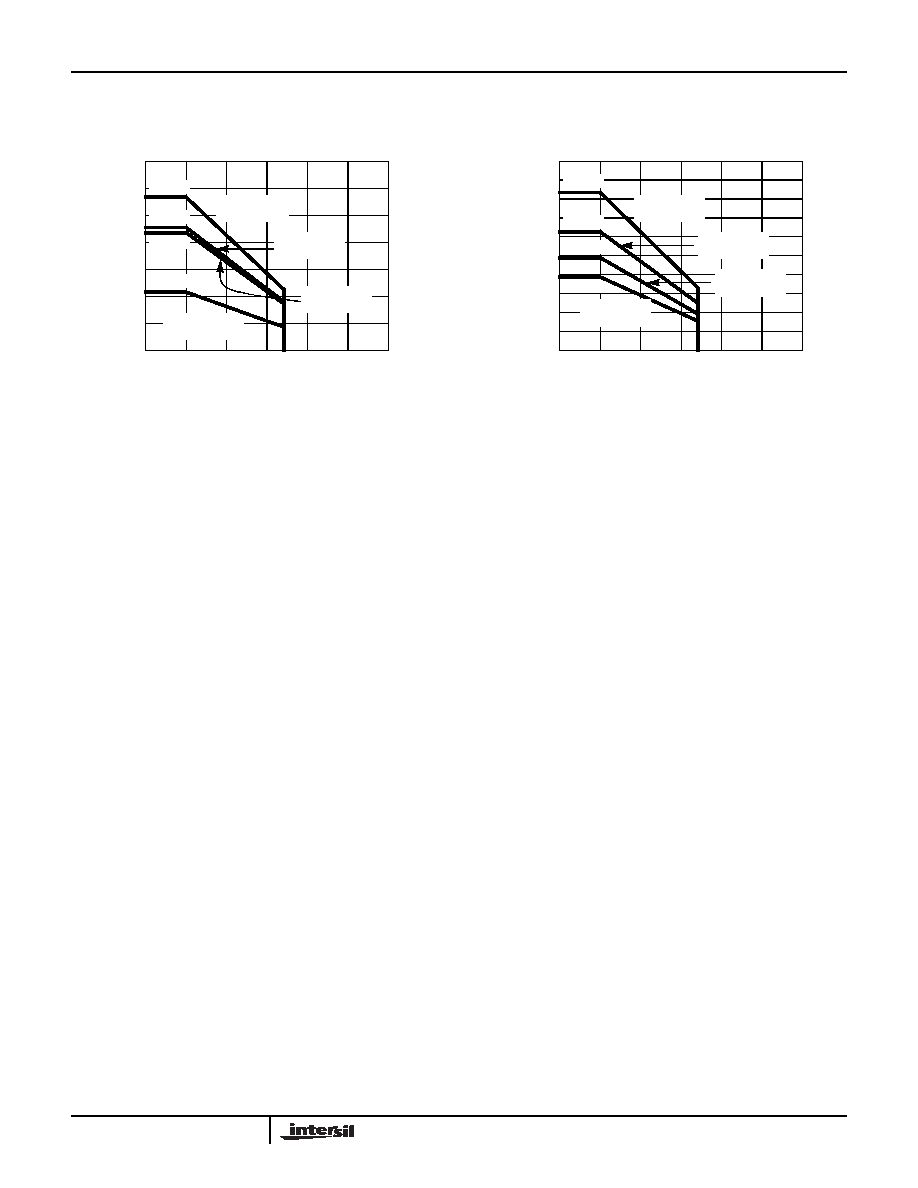
FIGURE 39.
PACKAGE POWER DISSIPATION vs AMBIENT
TEMPERATURE
FIGURE 40.
PACKAGE POWER DISSIPATION vs AMBIENT
TEMPERATURE
Typical Performance Curves (Continued)
JEDEC JESD51-7 HIGH EFFECTIVE THERMAL
CONDUCTIVITY TEST BOARD
1.136W
909mW
870mW
435mW
0
150
50
1.4
1.2
0.4
0
POWE
R
DI
SSP
IA
TIO
N
(W)
AMBIENT TEMPERATURE (°C)
0.2
125
25
0.8
100
75 85
1.0
0.6
θJA = 88°C/W
SO14
θJA = 230°C/W
SOT23-5/6
θJA = 110°C/W
SO8
θJA = 115°C/W
MSOP8/10
JEDEC JESD51-3 LOW EFFECTIVE THERMAL
CONDUCTIVITY TEST BOARD
0
150
50
1
0.9
0.2
0
POWE
R
DI
SSP
IA
TIO
N
(W)
AMBIENT TEMPERATURE (°C)
0.1
125
25
0.5
100
75 85
0.7
0.3
0.8
0.4
0.6
833mW
625mW
486mW
391mW
θJA = 265°C/W
SOT23-5/6
θJA = 206°C/W
MSOP8/10
θJA = 120°C/W
SO14
θJA = 160°C/W
SO8
EL5150, EL5151, EL5250, EL5251, EL5451
相关PDF资料 |
PDF描述 |
|---|---|
| EL5150IW-T7 | IC OP AMP LO OFF 200MHZ SOT23-6 |
| ISL28006FH20Z-T7A | IC OPAMP CURRENT SENSE SOT23-5 |
| LT1999HS8-50#TRPBF | IC AMP CURR SENSE HV 8-SOIC |
| MMS-117-01-L-DH | CONN RCPT 2MM 34POS DL HORZ PCB |
| SSQ 3 | FUSE 3A 125V 6125 FAST SSQ |
相关代理商/技术参数 |
参数描述 |
|---|---|
| EL5151IW-T7A | 功能描述:IC OP AMP LO OFF 200MHZ SOT-23-5 RoHS:否 类别:集成电路 (IC) >> Linear - Amplifiers - Instrumentation 系列:- 标准包装:1,000 系列:- 放大器类型:电压反馈 电路数:4 输出类型:满摆幅 转换速率:33 V/µs 增益带宽积:20MHz -3db带宽:30MHz 电流 - 输入偏压:2nA 电压 - 输入偏移:3000µV 电流 - 电源:2.5mA 电流 - 输出 / 通道:30mA 电压 - 电源,单路/双路(±):4.5 V ~ 16.5 V,±2.25 V ~ 8.25 V 工作温度:-40°C ~ 85°C 安装类型:表面贴装 封装/外壳:14-SOIC(0.154",3.90mm 宽) 供应商设备封装:14-SOIC 包装:带卷 (TR) |
| EL5151IWZ-T7 | 功能描述:IC AMP VFA SINGLE 200MHZ SOT23-5 RoHS:是 类别:集成电路 (IC) >> Linear - Amplifiers - Instrumentation 系列:- 标准包装:50 系列:- 放大器类型:通用 电路数:2 输出类型:满摆幅 转换速率:1.8 V/µs 增益带宽积:6.5MHz -3db带宽:4.5MHz 电流 - 输入偏压:5nA 电压 - 输入偏移:100µV 电流 - 电源:65µA 电流 - 输出 / 通道:35mA 电压 - 电源,单路/双路(±):1.8 V ~ 5.25 V,±0.9 V ~ 2.625 V 工作温度:-40°C ~ 85°C 安装类型:表面贴装 封装/外壳:10-TFSOP,10-MSOP(0.118",3.00mm 宽) 供应商设备封装:10-MSOP 包装:管件 |
| EL5151IWZ-T7A | 功能描述:IC AMP VFA SGL 200MHZ SOT23-5 RoHS:是 类别:集成电路 (IC) >> Linear - Amplifiers - Instrumentation 系列:- 标准包装:50 系列:- 放大器类型:通用 电路数:2 输出类型:满摆幅 转换速率:1.8 V/µs 增益带宽积:6.5MHz -3db带宽:4.5MHz 电流 - 输入偏压:5nA 电压 - 输入偏移:100µV 电流 - 电源:65µA 电流 - 输出 / 通道:35mA 电压 - 电源,单路/双路(±):1.8 V ~ 5.25 V,±0.9 V ~ 2.625 V 工作温度:-40°C ~ 85°C 安装类型:表面贴装 封装/外壳:10-TFSOP,10-MSOP(0.118",3.00mm 宽) 供应商设备封装:10-MSOP 包装:管件 |
| EL5152 | 制造商:INTERSIL 制造商全称:Intersil Corporation 功能描述:300MHz Amplifiers |
| EL5152_05 | 制造商:INTERSIL 制造商全称:Intersil Corporation 功能描述:270MHz Ultra-Accurate Amplifiers |
发布紧急采购,3分钟左右您将得到回复。