参数资料
| 型号: | EL5172IYZ-T13 |
| 厂商: | Intersil |
| 文件页数: | 2/15页 |
| 文件大小: | 0K |
| 描述: | IC LINE RCVR SGL 250MHZ 8-MSOP |
| 标准包装: | 2,500 |
| 放大器类型: | 差分 |
| 电路数: | 1 |
| 转换速率: | 800 V/µs |
| 增益带宽积: | 100MHz |
| -3db带宽: | 250MHz |
| 电流 - 输入偏压: | 6µA |
| 电压 - 输入偏移: | 7000µV |
| 电流 - 电源: | 5.6mA |
| 电流 - 输出 / 通道: | 95mA |
| 电压 - 电源,单路/双路(±): | 4.75 V ~ 11 V,±2.38 V ~ 5.5 V |
| 工作温度: | -40°C ~ 85°C |
| 安装类型: | 表面贴装 |
| 封装/外壳: | 8-TSSOP,8-MSOP(0.118",3.00mm 宽) |
| 供应商设备封装: | 8-MSOP |
| 包装: | 带卷 (TR) |
10
FN7311.10
September 4, 2012
Description of Operation and Application
Information
Product Description
The EL5172 and EL5372 are wide bandwidth, low power
and single/differential ended to single-ended output
amplifiers. The EL5172 is a single channel differential to
single-ended amplifier. The EL5372 is a triple channel
differential to single-ended amplifier. The EL5172 and
EL5372 are internally compensated for closed loop gain of
+1 or greater. Connected in gain of 1 and driving a 500
load, the EL5172 and EL5372 have a -3dB bandwidth of
250MHz. Driving a 150
load at gain of 2, the bandwidth is
about 50MHz. The bandwidth at the REF input is about
450MHz. The EL5172 and EL5372 are available with a
power-down feature to reduce the power while the amplifier
is disabled.
Input, Output and Supply Voltage Range
The EL5172 and EL5372 have been designed to operate
with a single supply voltage of 5V to 10V or split supplies
with its total voltage from 5V to 10V. The amplifiers have an
input common mode voltage range from -4.3V to 3.3V for
±5V supply. The differential mode input range (DMIR)
between the two inputs is about from -2.3V to +2.3V. The
input voltage range at the REF pin is from -3.6V to 3.3V. If
the input common mode or differential mode signal is outside
the above-specified ranges, it will cause the output signal to
be distorted.
The output of the EL5172 and EL5372 can swing from -3.8V
to 3.6V at 500
load at ±5V supply. As the load resistance
becomes lower, the output swing is reduced respectively.
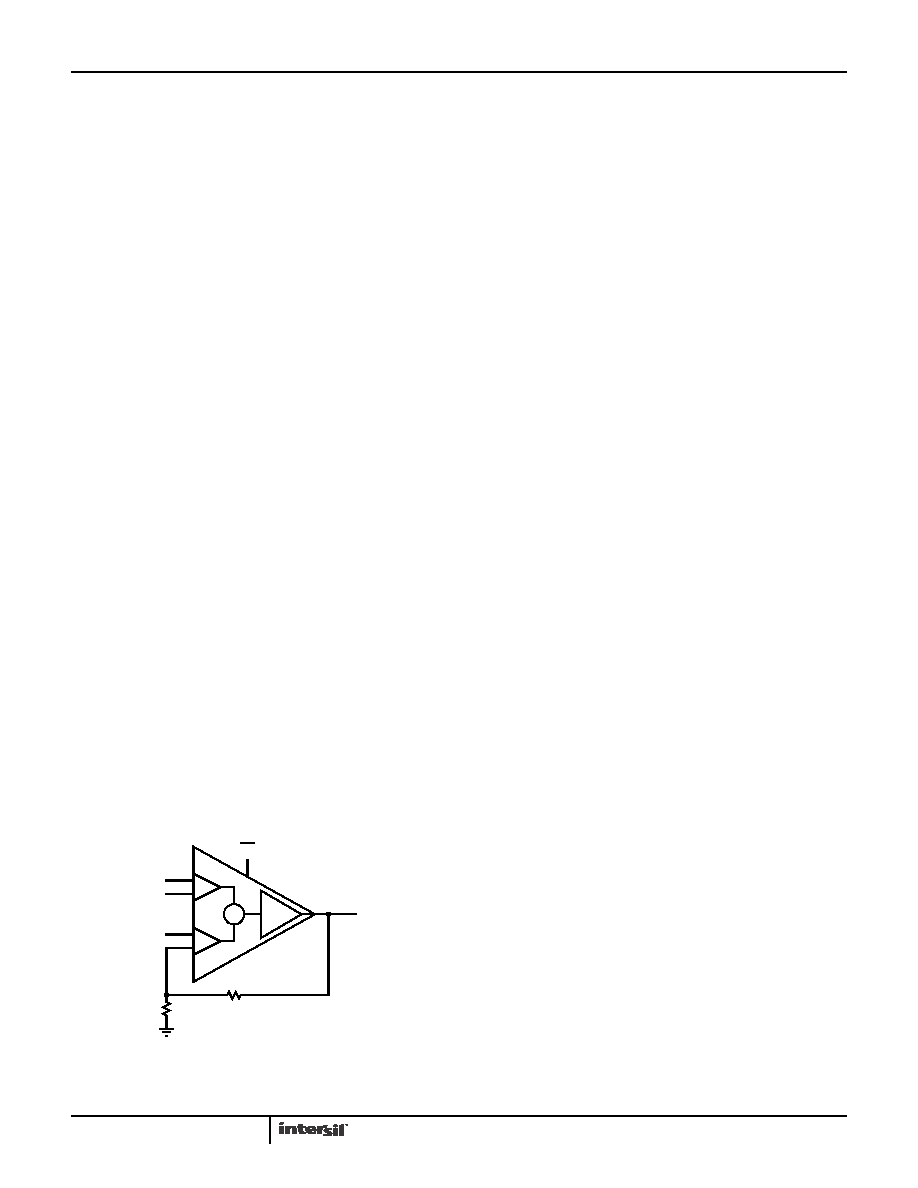
Overall Gain Settings
The gain setting for the EL5172 and the EL5372 is similar to
the conventional operational amplifier. The output voltage is
equal to the difference of the inputs plus VREF and then
times the gain, as expressed in Equation 1.
FIGURE 23.
Choice of Feedback Resistor and Gain Bandwidth
Product
For applications that require a gain of +1, no feedback
resistor is required; just short the OUT pin to the FB pin. For
gains greater than +1, the feedback resistor forms a pole
with the parasitic capacitance at the inverting input. As this
pole becomes smaller, the amplifier's phase margin is
reduced. This causes ringing in the time domain and
peaking in the frequency domain. Therefore, RF has some
maximum value that should not be exceeded for optimum
performance. If a large value of RF must be used, a small
capacitor in the few Pico farad range in parallel with RF can
help to reduce the ringing and peaking at the expense of
reducing the bandwidth.
The bandwidth of the EL5172 and EL5372 depends on the
load and the feedback network. RF and RG appear in
parallel with the load for gains other than +1. As this
combination gets smaller, the bandwidth falls off.
Consequently, RF also has a minimum value that should not
be exceeded for optimum bandwidth performance. For a
gain of +1, RF = 0 is optimum. For the gains other than +1,
optimum response is obtained with RF between 500 to
1k
. For AV = 2 and RF = RG = 1k, the BW is about 80MHz
and the frequency response is very flat.
The EL5172 and EL5372 have a gain bandwidth product of
100MHz. For gains
5, its bandwidth can be predicted using
Equation 2:
Driving Capacitive Loads and Cables
The EL5172 and EL5372 can drive 56pF capacitance in
parallel with 500
load to ground with 4dB of peaking at a
gain of +1. If less peaking is desired in applications, a small
series resistor (usually between 5
to 50) can be placed in
series with each output to eliminate most peaking. However,
this will reduce the gain slightly. If the gain setting is greater
than 1, the gain resistor RG can then be chosen to make-up
for any gain loss which may be created by the additional
series resistor at the output.
When used as a cable driver, double termination is always
recommended for reflection-free performance. For those
applications, a back-termination series resistor at the
amplifier's output will isolate the amplifier from the cable and
allow extensive capacitive drive. However, other applications
may have high capacitive loads without a back-termination
resistor. Again, a small series resistor at the output can help
to reduce peaking.
Disable/Power-Down
The EL5172 and EL5372 can be disabled and its outputs
placed in a high impedance state. The turn-off time is about
1.4s and the turn-on time is about 150ns. When disabled,
the amplifier's supply current is reduced to 80A for IS+ and
120A for IS- typically, thereby effectively eliminating the
V
O
V
IN +VIN -VREF
+
1
R
F
R
G
--------
+
–
=
(EQ. 1)
-
+
-
+
G/B
VO
EN
VIN+
VIN-
VREF
FB
RG
RF
Gain
BW
100MHz
=
(EQ. 2)
EL5172, EL5372
相关PDF资料 |
PDF描述 |
|---|---|
| 640919-2 | CONN RECEPT FASTON 14-16AWG .187 |
| SMBJ45CA | TVS BIDIRECT 600W 45V SMB |
| EL5172ISZ-T7 | IC LINE RCVR SGL 250MHZ 8-SOIC |
| SMBJ78CA | TVS BIDIRECT 600W 78V SMB |
| CRCW04029R53FKED | RES 9.53 OHM 1/16W 1% 0402 SMD |
相关代理商/技术参数 |
参数描述 |
|---|---|
| EL5172IYZ-T7 | 功能描述:差分放大器 EL5172IYZ 200MHZ DIFFERNTCVR RoHS:否 制造商:Texas Instruments 通道数量:1 Channel 带宽:2.4 GHz 可用增益调整:6 dB to 26 dB 输入补偿电压: 共模抑制比(最小值):- 40 dB 工作电源电压:4.75 V to 5.25 V 电源电流:100 mA 最大工作温度:+ 85 C 最小工作温度:- 40 C 安装风格:SMD/SMT 封装 / 箱体:WQFN-24 封装:Reel |
| EL5173IS | 功能描述:IC DRIVER DIFF 450MHZ TP 8-SOIC RoHS:否 类别:集成电路 (IC) >> Linear - Amplifiers - Instrumentation 系列:- 标准包装:1,000 系列:- 放大器类型:电压反馈 电路数:4 输出类型:满摆幅 转换速率:33 V/µs 增益带宽积:20MHz -3db带宽:30MHz 电流 - 输入偏压:2nA 电压 - 输入偏移:3000µV 电流 - 电源:2.5mA 电流 - 输出 / 通道:30mA 电压 - 电源,单路/双路(±):4.5 V ~ 16.5 V,±2.25 V ~ 8.25 V 工作温度:-40°C ~ 85°C 安装类型:表面贴装 封装/外壳:14-SOIC(0.154",3.90mm 宽) 供应商设备封装:14-SOIC 包装:带卷 (TR) |
| EL5173IS-T13 | 功能描述:IC DRIVER SGL 450MHZ DIFF 8-SOIC RoHS:否 类别:集成电路 (IC) >> Linear - Amplifiers - Instrumentation 系列:- 标准包装:50 系列:- 放大器类型:通用 电路数:2 输出类型:满摆幅 转换速率:1.8 V/µs 增益带宽积:6.5MHz -3db带宽:4.5MHz 电流 - 输入偏压:5nA 电压 - 输入偏移:100µV 电流 - 电源:65µA 电流 - 输出 / 通道:35mA 电压 - 电源,单路/双路(±):1.8 V ~ 5.25 V,±0.9 V ~ 2.625 V 工作温度:-40°C ~ 85°C 安装类型:表面贴装 封装/外壳:10-TFSOP,10-MSOP(0.118",3.00mm 宽) 供应商设备封装:10-MSOP 包装:管件 |
| EL5173IS-T7 | 功能描述:IC DRIVER DIFF 450MHZ TP 8-SOIC RoHS:否 类别:集成电路 (IC) >> Linear - Amplifiers - Instrumentation 系列:- 标准包装:1,000 系列:- 放大器类型:电压反馈 电路数:4 输出类型:满摆幅 转换速率:33 V/µs 增益带宽积:20MHz -3db带宽:30MHz 电流 - 输入偏压:2nA 电压 - 输入偏移:3000µV 电流 - 电源:2.5mA 电流 - 输出 / 通道:30mA 电压 - 电源,单路/双路(±):4.5 V ~ 16.5 V,±2.25 V ~ 8.25 V 工作温度:-40°C ~ 85°C 安装类型:表面贴装 封装/外壳:14-SOIC(0.154",3.90mm 宽) 供应商设备封装:14-SOIC 包装:带卷 (TR) |
| EL5173ISZ | 功能描述:差分放大器 EL5173ISZ 500MHZ DIFF DRVR GAIN=2 RoHS:否 制造商:Texas Instruments 通道数量:1 Channel 带宽:2.4 GHz 可用增益调整:6 dB to 26 dB 输入补偿电压: 共模抑制比(最小值):- 40 dB 工作电源电压:4.75 V to 5.25 V 电源电流:100 mA 最大工作温度:+ 85 C 最小工作温度:- 40 C 安装风格:SMD/SMT 封装 / 箱体:WQFN-24 封装:Reel |
发布紧急采购,3分钟左右您将得到回复。