参数资料
| 型号: | EL5210CY-T13 |
| 厂商: | Intersil |
| 文件页数: | 4/16页 |
| 文件大小: | 0K |
| 描述: | IC AMP DUAL R-R I/O 30MHZ 8-MSOP |
| 标准包装: | 2,500 |
| 放大器类型: | 电压反馈 |
| 电路数: | 2 |
| 输出类型: | 满摆幅 |
| 转换速率: | 33 V/µs |
| 增益带宽积: | 20MHz |
| -3db带宽: | 30MHz |
| 电流 - 输入偏压: | 2nA |
| 电压 - 输入偏移: | 3000µV |
| 电流 - 电源: | 2.5mA |
| 电流 - 输出 / 通道: | 30mA |
| 电压 - 电源,单路/双路(±): | 4.5 V ~ 16.5 V,±2.25 V ~ 8.25 V |
| 工作温度: | -40°C ~ 85°C |
| 安装类型: | 表面贴装 |
| 封装/外壳: | 10-TFSOP,10-MSOP(0.118",3.00mm 宽) |
| 供应商设备封装: | 8-MSOP |
| 包装: | 带卷 (TR) |
12
FN7185.3
July 5, 2007
when sourcing, and
when sinking.
Where:
i = 1 to 2 for Dual and 1 to 4 for Quad
VS = Total Supply Voltage
ISMAX = Maximum Supply Current Per Amplifier
VOUTi = Maximum Output Voltage of the Application
ILOADi = Load current
If we set the two PDMAX equations equal to each other, we
can solve for RLOADi to avoid device overheat. Figure 3 and
Figure 4 provide a convenient way to see if the device will
overheat. The maximum safe power dissipation can be
found graphically, based on the package type and the
ambient temperature. By using the previous equation, it is a
simple matter to see if PDMAX exceeds the device's power
derating curves. To ensure proper operation, it is important
to observe the recommended derating curves shown in
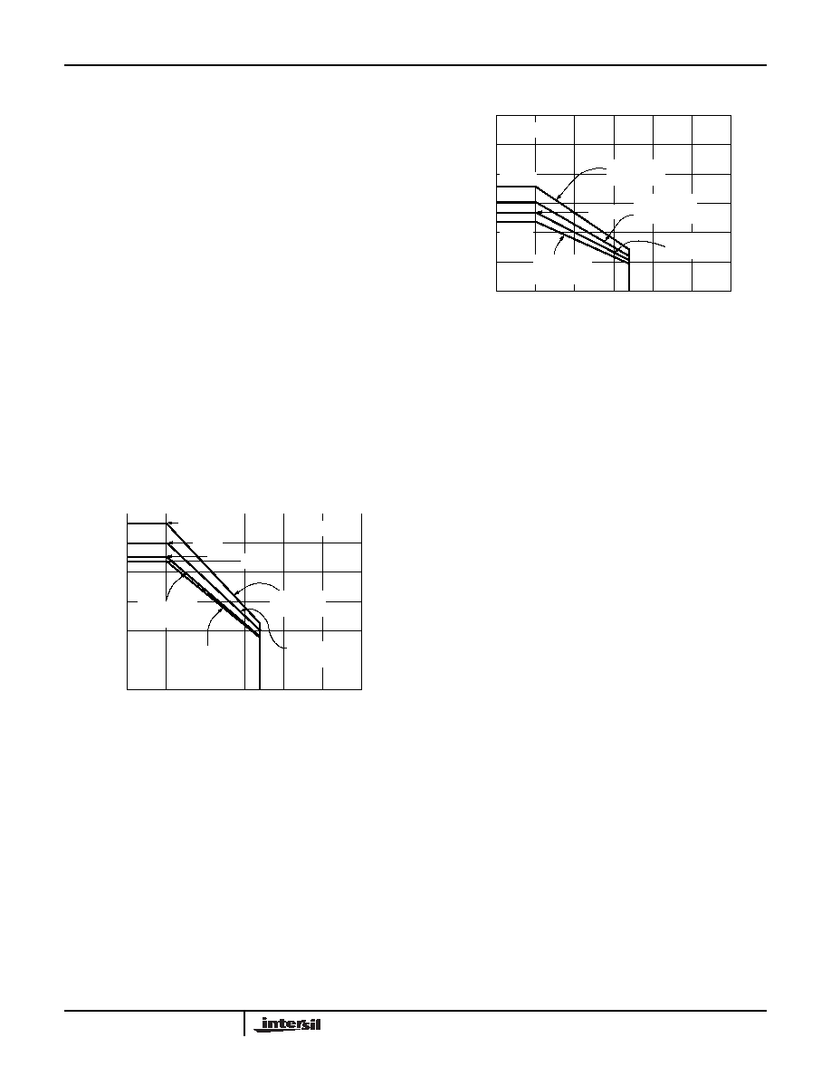
FIGURE 3. PACKAGE POWER DISSIPATION vs AMBIENT
TEMPERATURE
FIGURE 4. PACKAGE POWER DISSIPATION vs AMBIENT
TEMPERATURE
Unused Amplifiers
It is recommended that any unused amplifiers in a dual and
a quad package be configured as a unity gain follower. The
inverting input should be directly connected to the output
and the non-inverting input tied to the ground plane.
Driving Capacitive Loads
The EL5210 and EL5410 can drive a wide range of
capacitive loads. As load capacitance increases, however,
the -3dB bandwidth of the device will decrease and the
peaking increase. The amplifiers drive 10pF loads in parallel
with 1k
Ω with just 1.2dB of peaking, and 100pF with 6.5dB of
peaking. If less peaking is desired in these applications, a
small series resistor (usually between 5
Ω and 50Ω) can be
placed in series with the output. However, this will obviously
reduce the gain slightly. Another method of reducing peaking
is to add a "snubber" circuit at the output. A snubber is a
shunt load consisting of a resistor in series with a capacitor.
Values of 150
Ω and 10nF are typical. The advantage of a
snubber is that it does not draw any DC load current or
reduce the gain.
Power Supply Bypassing and Printed Circuit
Board Layout
The EL5210 and EL5410 can provide gain at high frequency.
As with any high-frequency device, good printed circuit
board layout is necessary for optimum performance. Ground
plane construction is highly recommended, lead lengths
should be as short as possible and the power supply pins
must be well bypassed to reduce the risk of oscillation. For
normal single supply operation, where the VS- pin is
connected to ground, a 0.1F ceramic capacitor should be
placed from VS+ to pin to VS- pin. A 4.7F tantalum
capacitor should then be connected in parallel, placed in the
region of the amplifier. One 4.7F capacitor may be used for
multiple devices. This same capacitor combination should be
placed at each supply pin to ground if split supplies are to be
used.
P
DMAX
ΣiV
[
S
I
SMAX
V
(
OUT iVS- )
I
LOADi
×
–
+
×]
=
50
150
400
800
P
o
wer
Diss
ipat
ion
(m
W
)
Ambient Temperature (°C)
0
100
0
1200
25
75
1000
600
200
125
85
MAX TJ=125°C
TSSOP14
θJA=100°C/W
SO8
θJA=110°C/W
Packages Mounted on a JEDEC JESD51-7 High Effective
Thermal Conductivity Test Board
1.0W
1.136W
909mW
833mW
SO14
θJA=88°C/W
MSOP8
θJA=115°C/W
50
150
400
800
P
o
we
rDi
ss
ip
ati
o
n
(m
W
)
Ambient Temperature (°C)
0
100
0125
1200
25
75
1000
600
200
85
MAX TJ=125°C
TSSOP14
θJA=165°C/W
SO8
θJA=160°C/W
MSOP8
θJA=206°C/W
SO14
θJA=120°C/W
Packages Mounted on a JEDEC JESD51-3 Low Effective
Thermal Conductivity Test Board
833mW
606mW
625mW
485mW
EL5210, EL5410
相关PDF资料 |
PDF描述 |
|---|---|
| PPPC371LGBN | CONN FEMALE 37POS .100" R/A GOLD |
| 3422.0047.11 | FUSE&HOLDER 1.5A 63V FAST SMD |
| 5-1676481-2 | RES 750 OHM 1/16W 0.1% 0603 |
| RT0603DRD071K1L | RES 1.1K OHM 1/10W .5% 0603 SMD |
| EL5210CSZ-T7 | IC AMP DUAL R-R I/O 30MHZ 8-SOIC |
相关代理商/技术参数 |
参数描述 |
|---|---|
| EL5210CY-T7 | 功能描述:IC OP AMP DUAL R-R 30MHZ 8-MSOP RoHS:否 类别:集成电路 (IC) >> Linear - Amplifiers - Instrumentation 系列:- 标准包装:1,000 系列:- 放大器类型:电压反馈 电路数:4 输出类型:满摆幅 转换速率:33 V/µs 增益带宽积:20MHz -3db带宽:30MHz 电流 - 输入偏压:2nA 电压 - 输入偏移:3000µV 电流 - 电源:2.5mA 电流 - 输出 / 通道:30mA 电压 - 电源,单路/双路(±):4.5 V ~ 16.5 V,±2.25 V ~ 8.25 V 工作温度:-40°C ~ 85°C 安装类型:表面贴装 封装/外壳:14-SOIC(0.154",3.90mm 宽) 供应商设备封装:14-SOIC 包装:带卷 (TR) |
| EL5210CYZ | 功能描述:IC OPAMP DUAL R-R I/O 8-MSOP RoHS:是 类别:集成电路 (IC) >> Linear - Amplifiers - Instrumentation 系列:- 标准包装:50 系列:- 放大器类型:通用 电路数:2 输出类型:满摆幅 转换速率:1.8 V/µs 增益带宽积:6.5MHz -3db带宽:4.5MHz 电流 - 输入偏压:5nA 电压 - 输入偏移:100µV 电流 - 电源:65µA 电流 - 输出 / 通道:35mA 电压 - 电源,单路/双路(±):1.8 V ~ 5.25 V,±0.9 V ~ 2.625 V 工作温度:-40°C ~ 85°C 安装类型:表面贴装 封装/外壳:10-TFSOP,10-MSOP(0.118",3.00mm 宽) 供应商设备封装:10-MSOP 包装:管件 |
| EL5210CYZ-T13 | 功能描述:IC AMP DUAL R-R I/O 30MHZ 8-MSOP RoHS:是 类别:集成电路 (IC) >> Linear - Amplifiers - Instrumentation 系列:- 标准包装:50 系列:- 放大器类型:通用 电路数:2 输出类型:满摆幅 转换速率:1.8 V/µs 增益带宽积:6.5MHz -3db带宽:4.5MHz 电流 - 输入偏压:5nA 电压 - 输入偏移:100µV 电流 - 电源:65µA 电流 - 输出 / 通道:35mA 电压 - 电源,单路/双路(±):1.8 V ~ 5.25 V,±0.9 V ~ 2.625 V 工作温度:-40°C ~ 85°C 安装类型:表面贴装 封装/外壳:10-TFSOP,10-MSOP(0.118",3.00mm 宽) 供应商设备封装:10-MSOP 包装:管件 |
| EL5210CYZ-T7 | 功能描述:IC AMP DUAL R-R I/O 30MHZ 8-MSOP RoHS:是 类别:集成电路 (IC) >> Linear - Amplifiers - Instrumentation 系列:- 标准包装:50 系列:- 放大器类型:通用 电路数:2 输出类型:满摆幅 转换速率:1.8 V/µs 增益带宽积:6.5MHz -3db带宽:4.5MHz 电流 - 输入偏压:5nA 电压 - 输入偏移:100µV 电流 - 电源:65µA 电流 - 输出 / 通道:35mA 电压 - 电源,单路/双路(±):1.8 V ~ 5.25 V,±0.9 V ~ 2.625 V 工作温度:-40°C ~ 85°C 安装类型:表面贴装 封装/外壳:10-TFSOP,10-MSOP(0.118",3.00mm 宽) 供应商设备封装:10-MSOP 包装:管件 |
| EL5211 | 制造商:INTERSIL 制造商全称:Intersil Corporation 功能描述:60MHz Rail-to-Rail Input-Output Op Amps |
发布紧急采购,3分钟左右您将得到回复。