参数资料
| 型号: | EL5220ILZ-T13 |
| 厂商: | Intersil |
| 文件页数: | 5/20页 |
| 文件大小: | 0K |
| 描述: | IC OPAMP RRIO 12MHZ 8-DFN |
| 标准包装: | 6,000 |
| 放大器类型: | 电压反馈 |
| 电路数: | 2 |
| 输出类型: | 满摆幅 |
| 转换速率: | 10 V/µs |
| 增益带宽积: | 8MHz |
| -3db带宽: | 12MHz |
| 电流 - 输入偏压: | 2nA |
| 电压 - 输入偏移: | 2000µV |
| 电流 - 电源: | 500µA |
| 电流 - 输出 / 通道: | 30mA |
| 电压 - 电源,单路/双路(±): | 4.5 V ~ 16.5 V,±2.25 V ~ 8.25 V |
| 工作温度: | -40°C ~ 85°C |
| 安装类型: | 表面贴装 |
| 封装/外壳: | 8-VFDFN 裸露焊盘 |
| 供应商设备封装: | 8-DFN(2x3) |
| 包装: | 带卷 (TR) |
13
All Intersil U.S. products are manufactured, assembled and tested utilizing ISO9000 quality systems.
Intersil Corporation’s quality certifications can be viewed at www.intersil.com/design/quality
Intersil products are sold by description only. Intersil Corporation reserves the right to make changes in circuit design, software and/or specifications at any time without
notice. Accordingly, the reader is cautioned to verify that data sheets are current before placing orders. Information furnished by Intersil is believed to be accurate and
reliable. However, no responsibility is assumed by Intersil or its subsidiaries for its use; nor for any infringements of patents or other rights of third parties which may result
from its use. No license is granted by implication or otherwise under any patent or patent rights of Intersil or its subsidiaries.
For information regarding Intersil Corporation and its products, see www.intersil.com
FN7186.7
December 15, 2011
supply voltage, plus the power in the IC due to the loads as
shown in Equation 2:
when sourcing, and:
when sinking.
where:
i = 1 to 2 for dual and 1 to 4 for quad
VS = Total supply voltage
ISMAX = Maximum supply current per amplifier
VOUTi = Maximum output voltage of the application
ILOADi = Load current
If we set the two PDMAX equations equal to each other, we
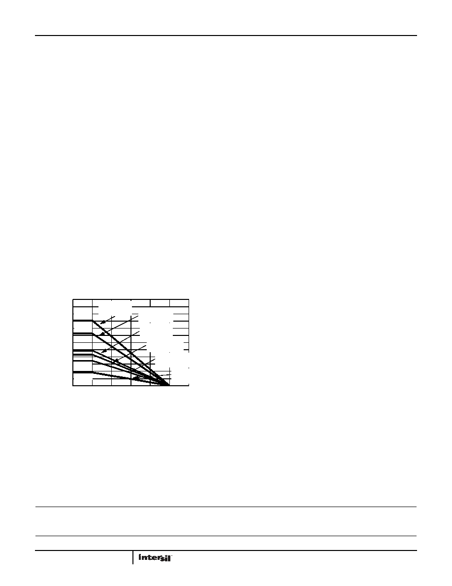
provide a convenient way to see if the device will overheat.
The maximum safe power dissipation can be found
graphically, based on the package type and the ambient
temperature. By using the previous equation, it is a simple
matter to see if PDMAX exceeds the device's power derating
curves. To ensure proper operation, it is important to observe
the recommended derating curves in Figure 27.
Unused Amplifiers
It is recommended that any unused amplifiers in a dual and
a quad package be configured as a unity gain follower. The
inverting input should be directly connected to the output
and the non-inverting input tied to the ground plane.
Driving Capacitive Loads
The EL5120, EL5220, and EL5420 can drive a wide range of
capacitive loads. As load capacitance increases, however,
the -3dB bandwidth of the device will decrease and the
peaking will increase. The amplifiers drive 10pF loads in
parallel with 10k
Ω with just 1.5dB of peaking, and 100pF
with 6.4dB of peaking. If less peaking is desired in these
applications, a small series resistor (usually between 5
Ω and
50
Ω) can be placed in series with the output. However, this
will obviously reduce the gain slightly. Another method of
reducing peaking is to add a “snubber” circuit at the output.
A snubber is a shunt load consisting of a resistor in series
with a capacitor. Values of 150
Ω and 10nF are typical. The
advantage of a snubber is that it does not draw any DC load
current or reduce the gain
Power Supply Bypassing and Printed Circuit
Board Layout
The EL5120, EL5220, and EL5420 can provide gain at high
frequency. As with any high-frequency device, good printed
circuit board layout is necessary for optimum performance.
Ground plane construction is highly recommended, lead
lengths should be as short as possible and the power supply
pins must be well bypassed to reduce the risk of oscillation.
For normal single supply operation, where the VS- pin is
connected to ground, a 0.1F ceramic capacitor should be
placed from VS+ to pin to VS- pin. A 4.7F tantalum
capacitor should then be connected in parallel, placed in the
region of the amplifier. One 4.7F capacitor may be used for
multiple devices. This same capacitor combination should be
placed at each supply pin to ground if split supplies are to be
used.
P
DMAX
ΣiV
S
I
SMAX
V
S+
(
V
OUT i )
I
LOAD i
×
–
+
×
[]
×
=
(EQ. 2)
P
DMAX
ΣiV
S
I
SMAX
V
OUTi
(
V
S- )
I
LOADi
×
–
+
×
[]
×
=
(EQ. 3)
0.0
0.5
1.0
1.5
2.0
2.5
3.0
0
25
50
75
100
125
150
FIGURE 27. PACKAGE POWER DISSIPATION vs AMBIENT
TEMPERATURE
JEDEC JESD51-7 HIGH EFFECTIVE THERMAL
CONDUCTIVITY TEST BOARD
POWER
DIS
S
IP
A
T
ION
(W
)
AMBIENT TEMPERATURE (°C)
θJA = 44°C/W
QFN16
2.27W
θJA = 55°C/W
DFN8
1.80W
1.22W
θ
JA = 82°C/W
SOIC14
467mW
870mW
θJA = 115°C/W
MSOP8
θJA = 93°C/W
TSSOP14
θJA = 214°C/W
TSOT5
EL5120, EL5220, EL5420
相关PDF资料 |
PDF描述 |
|---|---|
| EL5220TIYZ-T7 | IC OPAMP GP R-R 12MHZ 8MSOP |
| EL5221CYZ-T7 | IC OPAMP DUAL R-R 12MHZ 8-MSOP |
| EL5236IYZ-T13 | IC OPAMP GP 300MHZ DUAL LN 8MSOP |
| EL5292CS-T7 | IC AMP CFA DUAL 600MHZ 8-SOIC |
| EL5293CSZ-T7 | IC AMP CFA DUAL 300MHZ 8-SOIC |
相关代理商/技术参数 |
参数描述 |
|---|---|
| EL5220T | 制造商:INTERSIL 制造商全称:Intersil Corporation 功能描述:12MHz Rail-to-Rail Input-Output Operational Amplifier |
| EL5220TILZ-T13 | 功能描述:运算放大器 - 运放 EL5220TILZ 12MHZ R2R R2R I/O OPERATE AMP RoHS:否 制造商:STMicroelectronics 通道数量:4 共模抑制比(最小值):63 dB 输入补偿电压:1 mV 输入偏流(最大值):10 pA 工作电源电压:2.7 V to 5.5 V 安装风格:SMD/SMT 封装 / 箱体:QFN-16 转换速度:0.89 V/us 关闭:No 输出电流:55 mA 最大工作温度:+ 125 C 封装:Reel |
| EL5220TIYZ | 功能描述:运算放大器 - 运放 EL5220TIYZ 12MHZ R2R INPUT-OUTPUT OPERATE RoHS:否 制造商:STMicroelectronics 通道数量:4 共模抑制比(最小值):63 dB 输入补偿电压:1 mV 输入偏流(最大值):10 pA 工作电源电压:2.7 V to 5.5 V 安装风格:SMD/SMT 封装 / 箱体:QFN-16 转换速度:0.89 V/us 关闭:No 输出电流:55 mA 最大工作温度:+ 125 C 封装:Reel |
| EL5220TIYZ-T13 | 功能描述:运算放大器 - 运放 EL5220TIYZ 12MHZ R2R INPUT-OUTPUT OPERATE RoHS:否 制造商:STMicroelectronics 通道数量:4 共模抑制比(最小值):63 dB 输入补偿电压:1 mV 输入偏流(最大值):10 pA 工作电源电压:2.7 V to 5.5 V 安装风格:SMD/SMT 封装 / 箱体:QFN-16 转换速度:0.89 V/us 关闭:No 输出电流:55 mA 最大工作温度:+ 125 C 封装:Reel |
| EL5220TIYZ-T7 | 功能描述:运算放大器 - 运放 EL5220TIYZ 12MHZ R2R INPUT-OUTPUT OPERATE RoHS:否 制造商:STMicroelectronics 通道数量:4 共模抑制比(最小值):63 dB 输入补偿电压:1 mV 输入偏流(最大值):10 pA 工作电源电压:2.7 V to 5.5 V 安装风格:SMD/SMT 封装 / 箱体:QFN-16 转换速度:0.89 V/us 关闭:No 输出电流:55 mA 最大工作温度:+ 125 C 封装:Reel |
发布紧急采购,3分钟左右您将得到回复。