参数资料
| 型号: | EL5224IL |
| 厂商: | Intersil |
| 文件页数: | 12/12页 |
| 文件大小: | 0K |
| 描述: | IC BUFFER LP 8-CH 12MHZ 24-QFN |
| 标准包装: | 90 |
| 放大器类型: | 缓冲器 |
| 电路数: | 8 |
| 输出类型: | 满摆幅 |
| 转换速率: | 15 V/µs |
| 增益带宽积: | 8MHz |
| -3db带宽: | 12MHz |
| 电流 - 输入偏压: | 2nA |
| 电压 - 输入偏移: | 2000µV |
| 电流 - 电源: | 6.8mA |
| 电流 - 输出 / 通道: | 140mA |
| 电压 - 电源,单路/双路(±): | 4.5 V ~ 16.5 V,±2.25 V ~ 8.25 V |
| 工作温度: | -40°C ~ 85°C |
| 安装类型: | 表面贴装 |
| 封装/外壳: | 24-VFQFN 裸露焊盘 |
| 供应商设备封装: | 24-QFN-EP |
| 包装: | 管件 |
9
UNUSED BUFFERS
It is recommended that any unused buffers have their inputs
tied to the ground plane.
DRIVING CAPACITIVE LOADS
The buffers can drive a wide range of capacitive loads. As
load capacitance increases, however, the -3dB bandwidth of
the device will decrease and the peaking increase. The
buffers drive 10pF loads in parallel with 10k
Ω with just 1.5dB
of peaking, and 100pF with 6.4dB of peaking. If less peaking
is desired in these applications, a small series resistor
(usually between 5
Ω and 50Ω) can be placed in series with
the output. However, this will obviously reduce the gain
slightly. Another method of reducing peaking is to add a
snubber circuit at the output. A snubber is a shunt load
consisting of a resistor in series with a capacitor. Values of
150
Ω and 10nF are typical. The advantage of a snubber is
that it does not draw any DC load current or reduce the gain.
The Use of VCOM Amplifier
The VCOM amplifier is designed to control the voltage on the
back plate of an LCD display. This plate is capacitively
coupled to the pixel drive voltage which alternately cycles
positive and negative at the line rate for the display. Thus the
amplifier must be capable of sourcing and sinking capacitive
pulses of current, which can occasionally be quite large (a
few 100mA for typical applications).
A simple use of the VCOM amplifier is as a voltage follower,
as illustrated in Figure 23. Here, a voltage, corresponding to
the mid-DAC potential, is generated by a resistive divider
and buffered by the amplifier. The amplifier's stability is
designed to be dominated by the load capacitance, thus for
very short duration pulses (< 1s) the output capacitor
supplies the current. For longer pulses the VCOM amplifier
supplies the current. By virtue of its high transconductance
which progressively increases as more current is drawn, it
can maintain regulation within 5mV as currents up to 100mA
are drawn, while consuming only 2mA of quiescent current.
Alternatively, the back plate potential can be generated by a
DAC and the VCOM amplifier used to buffer the DAC
voltage, with gain if necessary. This is shown in Figure 24. In
this case, the effective transconductance of the feedback is
reduced, thus the amplifier will be more stable, but regulation
will be degraded by the feedback factor.
CHOICE OF OUTPUT CAPACITOR
A 1F ceramic capacitor with low ESR is recommended for
this amplifier. (For example, GRM42_ 6X7R105K16). This
capacitor determines the stability of the amplifier. Reducing it
will make the amplifier less stable, and should be avoided.
With a 1F capacitor, the unity gain bandwidth of the
amplifier is close to 1MHz when reasonable currents are
being drawn. (For lower load currents, the gain and hence
bandwidth progressively decreases.) This means the active
trans-conductance is:
This high transconductance indicates why it is important to
have a low ESR capacitor.
If:
then the capacitor will not force the gain to roll off below
unity, and subsequent poles can affect stability. The
recommended capacitor has an ESR of 10m
Ω, but to this
must be added the resistance of the board trace between the
capacitor and the sense connection - therefore this should
be kept short, as illustrated in Figure 21, by the diagonal line
to the capacitor. Also ground resistance between the
capacitor and the base of R2 must be kept to a minimum.
These constraints should be considered when laying out the
PCB.
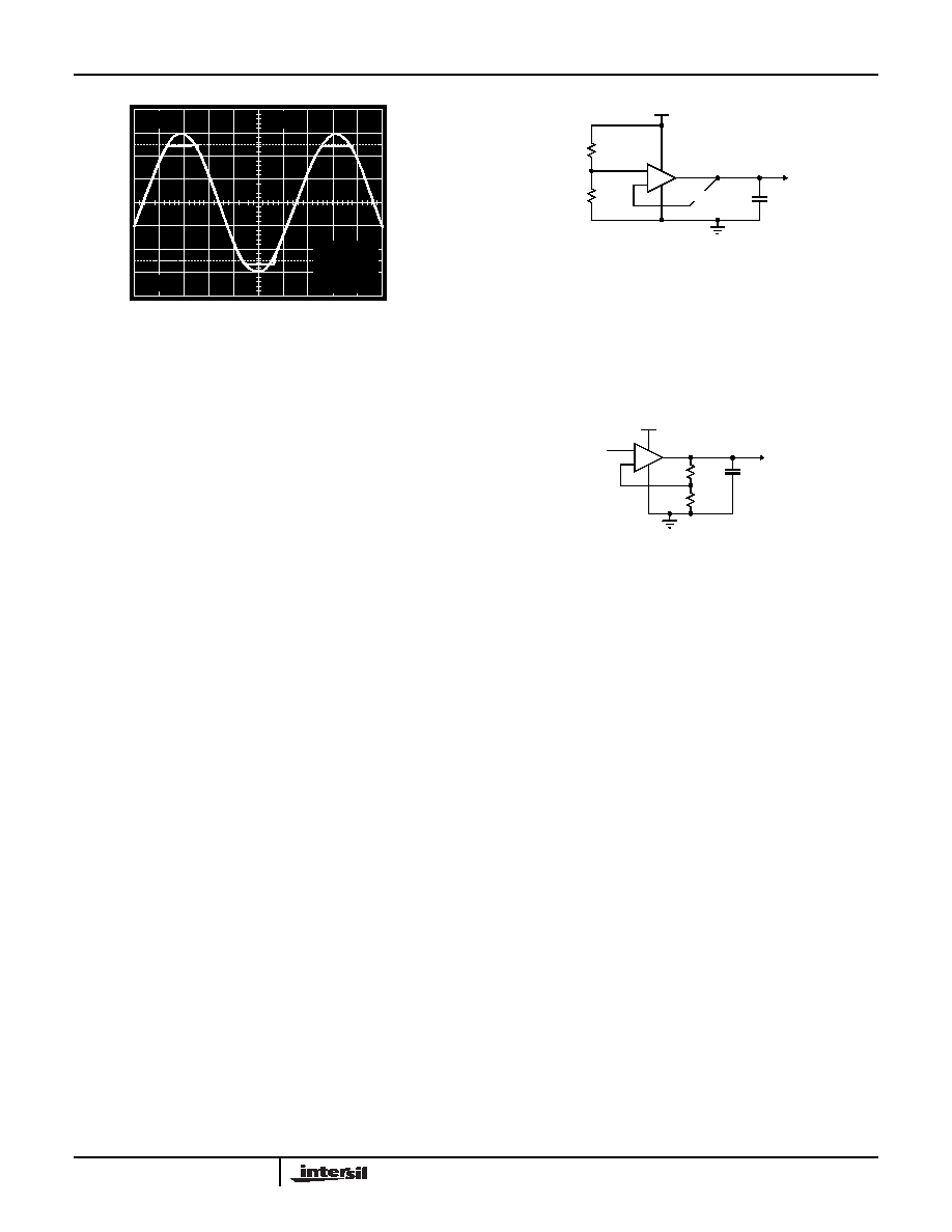
1V
10s
VS=±2.5V
TA=25°C
VIN=6VP-P
FIGURE 22. OPERATION WITH BEYOND-THE-RAILS INPUT
-
+
R1
R2
VBOOST
VCOM
1F CERAMIC
LOW ESR
IPCOM
INCOM
VCOM
VDDCOM
FIGURE 23. VCOM USED AS A VOLTAGE BUFFER
VSSCOM
-
+
R1
R2
VBOOST
VCOM
1F CERAMIC
LOW ESR
FROM DAC
FIGURE 24. VCOM USED AS A BUFFER WITH GAIN
2
π 1μF1MHz
×
6.28S
=
ESR
6.28
1
>
×
EL5224, EL5324, EL5424
相关PDF资料 |
PDF描述 |
|---|---|
| 0034.3779 | FUSE 2A 250VAC 5X20 SLOW |
| EL5223CR-T7 | IC OPAMP OCTAL R-R 12MHZ 20TSSOP |
| 0034.3776 | FUSE 1.25A 250VAC 5X20 SLOW |
| EL5223CR-T13 | IC OPAMP OCTAL R-R 12MHZ 20TSSOP |
| 0034.3882 | FUSE 3.5A 250VAC 5X20 FAST |
相关代理商/技术参数 |
参数描述 |
|---|---|
| EL5224IL-T13 | 功能描述:IC BUFFER LP 8-CH 12MHZ 24-QFN RoHS:否 类别:集成电路 (IC) >> Linear - Amplifiers - Instrumentation 系列:- 标准包装:50 系列:- 放大器类型:通用 电路数:2 输出类型:满摆幅 转换速率:1.8 V/µs 增益带宽积:6.5MHz -3db带宽:4.5MHz 电流 - 输入偏压:5nA 电压 - 输入偏移:100µV 电流 - 电源:65µA 电流 - 输出 / 通道:35mA 电压 - 电源,单路/双路(±):1.8 V ~ 5.25 V,±0.9 V ~ 2.625 V 工作温度:-40°C ~ 85°C 安装类型:表面贴装 封装/外壳:10-TFSOP,10-MSOP(0.118",3.00mm 宽) 供应商设备封装:10-MSOP 包装:管件 |
| EL5224IL-T7 | 功能描述:IC BUFFER LP 8-CH 12MHZ 24-QFN RoHS:否 类别:集成电路 (IC) >> Linear - Amplifiers - Instrumentation 系列:- 标准包装:50 系列:- 放大器类型:通用 电路数:2 输出类型:满摆幅 转换速率:1.8 V/µs 增益带宽积:6.5MHz -3db带宽:4.5MHz 电流 - 输入偏压:5nA 电压 - 输入偏移:100µV 电流 - 电源:65µA 电流 - 输出 / 通道:35mA 电压 - 电源,单路/双路(±):1.8 V ~ 5.25 V,±0.9 V ~ 2.625 V 工作温度:-40°C ~ 85°C 安装类型:表面贴装 封装/外壳:10-TFSOP,10-MSOP(0.118",3.00mm 宽) 供应商设备封装:10-MSOP 包装:管件 |
| EL5224ILZ | 功能描述:运算放大器 - 运放 EL5224ILZ 12MHZ R2R BUFR W/VCOM AMP RoHS:否 制造商:STMicroelectronics 通道数量:4 共模抑制比(最小值):63 dB 输入补偿电压:1 mV 输入偏流(最大值):10 pA 工作电源电压:2.7 V to 5.5 V 安装风格:SMD/SMT 封装 / 箱体:QFN-16 转换速度:0.89 V/us 关闭:No 输出电流:55 mA 最大工作温度:+ 125 C 封装:Reel |
| EL5224ILZ-T13 | 功能描述:运算放大器 - 运放 EL5224ILZ 12MHZ R2R BUFR W/VCOM AMP RoHS:否 制造商:STMicroelectronics 通道数量:4 共模抑制比(最小值):63 dB 输入补偿电压:1 mV 输入偏流(最大值):10 pA 工作电源电压:2.7 V to 5.5 V 安装风格:SMD/SMT 封装 / 箱体:QFN-16 转换速度:0.89 V/us 关闭:No 输出电流:55 mA 最大工作温度:+ 125 C 封装:Reel |
| EL5224ILZ-T7 | 功能描述:运算放大器 - 运放 EL5224ILZ 12MHZ R2R BUFR W/VCOM AMP RoHS:否 制造商:STMicroelectronics 通道数量:4 共模抑制比(最小值):63 dB 输入补偿电压:1 mV 输入偏流(最大值):10 pA 工作电源电压:2.7 V to 5.5 V 安装风格:SMD/SMT 封装 / 箱体:QFN-16 转换速度:0.89 V/us 关闭:No 输出电流:55 mA 最大工作温度:+ 125 C 封装:Reel |
发布紧急采购,3分钟左右您将得到回复。