参数资料
| 型号: | EL5236IYZ-T13 |
| 厂商: | Intersil |
| 文件页数: | 5/19页 |
| 文件大小: | 0K |
| 描述: | IC OPAMP GP 300MHZ DUAL LN 8MSOP |
| 标准包装: | 2,500 |
| 放大器类型: | 电压反馈 |
| 电路数: | 2 |
| 转换速率: | 128 V/µs |
| 增益带宽积: | 300MHz |
| -3db带宽: | 250MHz |
| 电流 - 输入偏压: | 6.5µA |
| 电压 - 输入偏移: | 100µV |
| 电流 - 电源: | 5.8mA |
| 电流 - 输出 / 通道: | 160mA |
| 电压 - 电源,单路/双路(±): | 5 V ~ 12 V,±2.5 V ~ 6 V |
| 工作温度: | -40°C ~ 85°C |
| 安装类型: | 表面贴装 |
| 封装/外壳: | 8-TSSOP,8-MSOP(0.118",3.00mm 宽) |
| 供应商设备封装: | 8-MSOP |
| 包装: | 带卷 (TR) |
EL5236, EL5237
13
FN7833.0
March 31, 2011
Applications Information
Non-inverting Operation
The dual wideband EL5236 (and EL5237 with disable) provides a
very power efficient low gain optimized amplifier solution using a
slightly decompensated VFA design. This gives a lower input
referred voltage noise and higher slew rate at the very low
5.6mA/ch nominal supply current. Unity gain operation is
possible with external compensation but most high speed
designs are at a gain > 1.
Figure 37 shows the gain of +2V/V configuration used for most of
the characterization curves. As most lab equipment is expecting
a 50 termination at the source, the non-inverting input and
output show a 50 termination. The 402 feedback and gain
resistors give a good compromise between several parasitic
factors. These include the added noise of those resistors, loading
effects, and to minimize the loss of phase margin back to the
inverting node. A wide range of values can be used, where lower
values will reduce noise with more output loading and higher
values will start to dominate the output noise and introduce
more phase margin loss into the loop. The EL5236 macromodel
is a very good tool to predict the impact of these different values.
varied the Rg element to achieve different gain settings.
Inverting Operation
Figure 38 shows the inverting gain configuration used for the
inverting mode characterization curves. In this case, the
feedback resistor is held at 402 while both the Rg and Rt
elements are adjusted. Rg is adjusted to get different gains while
Rt is adjusted to retain the input impedance at 50. This does
give a different loop gain (and hence bandwidth vs. gain) profile
over gain as reflected in Figure 39. In a system application, Rm
can be used to match the source impedance to get bias current
cancellation. For the lowest noise, include a de-coupling
capacitor across that resistor (0.1F in Figure 38).
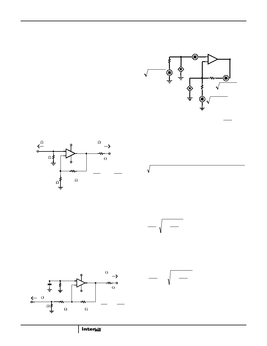
Getting the Lowest Noise
A very low noise op amp like the EL5236 will only deliver a low
output noise if the resistor values used to implement the design
add a noise contribution that is also low. Figure 39 shows the full
noise model for a non-inverting configuration.
Each of these voltage and current noise terms will contribute to
an output noise power. Getting the gains for each, then squaring,
summing, and then taking the square root will give the combined
output spot noise using the model of Figure 39 as shown in
Equation 1:
The source resistor shows up combining with the op amps
non-inverting input voltage noise to give a total non-inverting
input noise that then gets the full noise gain to the output. As a
point of reference, solve for where those noise terms equal the
contribution from just the op amp voltage noise. This is given in
Equation 2 and evaluating this for the 1.5nV and 1.8pA input
noise terms gives Rs = 136.
Similarly, compare the output noise due to just the non-inverting
input noise voltage to the terms on the inverting node in
Equation 1. Solving for equality there (to get a maximum Rf value
to limit the inverting side noise contributions at the output), gives
Equation 3. Evaluating this for 1.5nV and 1.8pA input noise
terms at a NG = 2 gives an Rf = 272.
This simplified analysis indicates the 402 used for the
non-inverting characterization is already starting to dominate the
output noise at a gain of 2. Going up in gain, with a fixed Rf = 402,
will quickly make those input side terms dominant.
-
+
50
402
Rg
50
+6V
ISL5236
Vo
Vi
-6V
Rf
50
LOAD
50
SOURCE
Rg
Rf
Vi
Vo
+
= 1
FIGURE 37. G = +2V/V CHARACTERIZATION CIRCUIT
-
+
Rm
402
Rg
50
+6V
ISL5236
Vo
Vi
-6V
Rf
50 LOAD
50
SOURCE
0.1F
57.6
Rg
Rf
Vi
Vo
=
FIGURE 38. G = -1V/V CHARACTERIZATION CIRCUIT
-
+
Rg
eo
Rs
Rf
iN
eN
ii
kTRs
4
kTRs
4
kTRs
4
Rg
Rf
NoiseGain
+
=1
FIGURE 39. OP AMP NON-INVERTING NOISE ANALYSIS CIRCUIT
()
(
) () ()
()
NG
kTR
R
i
NG
kTR
R
i
e
f
i
s
n
o
4
2
+
+
=
(EQ. 1)
+
=
1
2
1
2
kT
i
e
i
kT
R
n
s
(EQ. 2)
+
=
1
2
1
2
kT
i
e
NG
i
kT
R
n
f
(EQ. 3)
相关PDF资料 |
PDF描述 |
|---|---|
| EL5292CS-T7 | IC AMP CFA DUAL 600MHZ 8-SOIC |
| EL5293CSZ-T7 | IC AMP CFA DUAL 300MHZ 8-SOIC |
| EL5308IUZ | IC AMP FGA TRPL 450MHZ 16-QSOP |
| EL5360IUZ-T13 | IC AMP CFA TRIPLE 200MHZ 16-QSOP |
| EL5362IUZ | IC AMP CFA TRIPLE 500MHZ 16-QSOP |
相关代理商/技术参数 |
参数描述 |
|---|---|
| EL5236IYZ-T7 | 功能描述:高速运算放大器 EL5236IYZ RoHS:否 制造商:Texas Instruments 通道数量:1 电压增益 dB:116 dB 输入补偿电压:0.5 mV 转换速度:55 V/us 工作电源电压:36 V 电源电流:7.5 mA 最大工作温度:+ 85 C 安装风格:SMD/SMT 封装 / 箱体:SOIC-8 封装:Tube |
| EL5237 | 制造商:INTERSIL 制造商全称:Intersil Corporation 功能描述:Dual Ultra Low Noise Wideband Amplifiers Voltage Noise: 1.5nV/a??Hz |
| EL5237IYZ | 功能描述:高速运算放大器 EL5237IYZ RoHS:否 制造商:Texas Instruments 通道数量:1 电压增益 dB:116 dB 输入补偿电压:0.5 mV 转换速度:55 V/us 工作电源电压:36 V 电源电流:7.5 mA 最大工作温度:+ 85 C 安装风格:SMD/SMT 封装 / 箱体:SOIC-8 封装:Tube |
| EL5237IYZ-T13 | 功能描述:高速运算放大器 EL5237IYZ RoHS:否 制造商:Texas Instruments 通道数量:1 电压增益 dB:116 dB 输入补偿电压:0.5 mV 转换速度:55 V/us 工作电源电压:36 V 电源电流:7.5 mA 最大工作温度:+ 85 C 安装风格:SMD/SMT 封装 / 箱体:SOIC-8 封装:Tube |
| EL5237IYZ-T7 | 功能描述:高速运算放大器 EL5237IYZ RoHS:否 制造商:Texas Instruments 通道数量:1 电压增益 dB:116 dB 输入补偿电压:0.5 mV 转换速度:55 V/us 工作电源电压:36 V 电源电流:7.5 mA 最大工作温度:+ 85 C 安装风格:SMD/SMT 封装 / 箱体:SOIC-8 封装:Tube |
发布紧急采购,3分钟左右您将得到回复。