参数资料
| 型号: | EL5375IU |
| 厂商: | Intersil |
| 文件页数: | 3/15页 |
| 文件大小: | 0K |
| 描述: | IC AMP TRPL DIFF 550MHZ 24-QSOP |
| 标准包装: | 55 |
| 放大器类型: | 差分 |
| 电路数: | 3 |
| 转换速率: | 900 V/µs |
| 增益带宽积: | 200MHz |
| -3db带宽: | 550MHz |
| 电流 - 输入偏压: | 12.5µA |
| 电压 - 输入偏移: | 3000µV |
| 电流 - 电源: | 9.6mA |
| 电流 - 输出 / 通道: | 67mA |
| 电压 - 电源,单路/双路(±): | 4.75 V ~ 11 V,±2.38 V ~ 5.5 V |
| 工作温度: | -40°C ~ 85°C |
| 安装类型: | 表面贴装 |
| 封装/外壳: | 24-SSOP(0.154",3.90mm 宽) |
| 供应商设备封装: | 24-QSOP |
| 包装: | 管件 |
11
FN7306.7
August 25, 2010
power consumption. The amplifier's power-down can be
controlled by standard CMOS signal levels at the ENABLE
pin. The applied logic signal is relative to the VS+ pin. Letting
the EN pin float or applying a signal that is less than 1.5V
below VS+ will enable the amplifier. The amplifier will be
disabled when the signal at the EN pin is above VS+ - 0.5V.
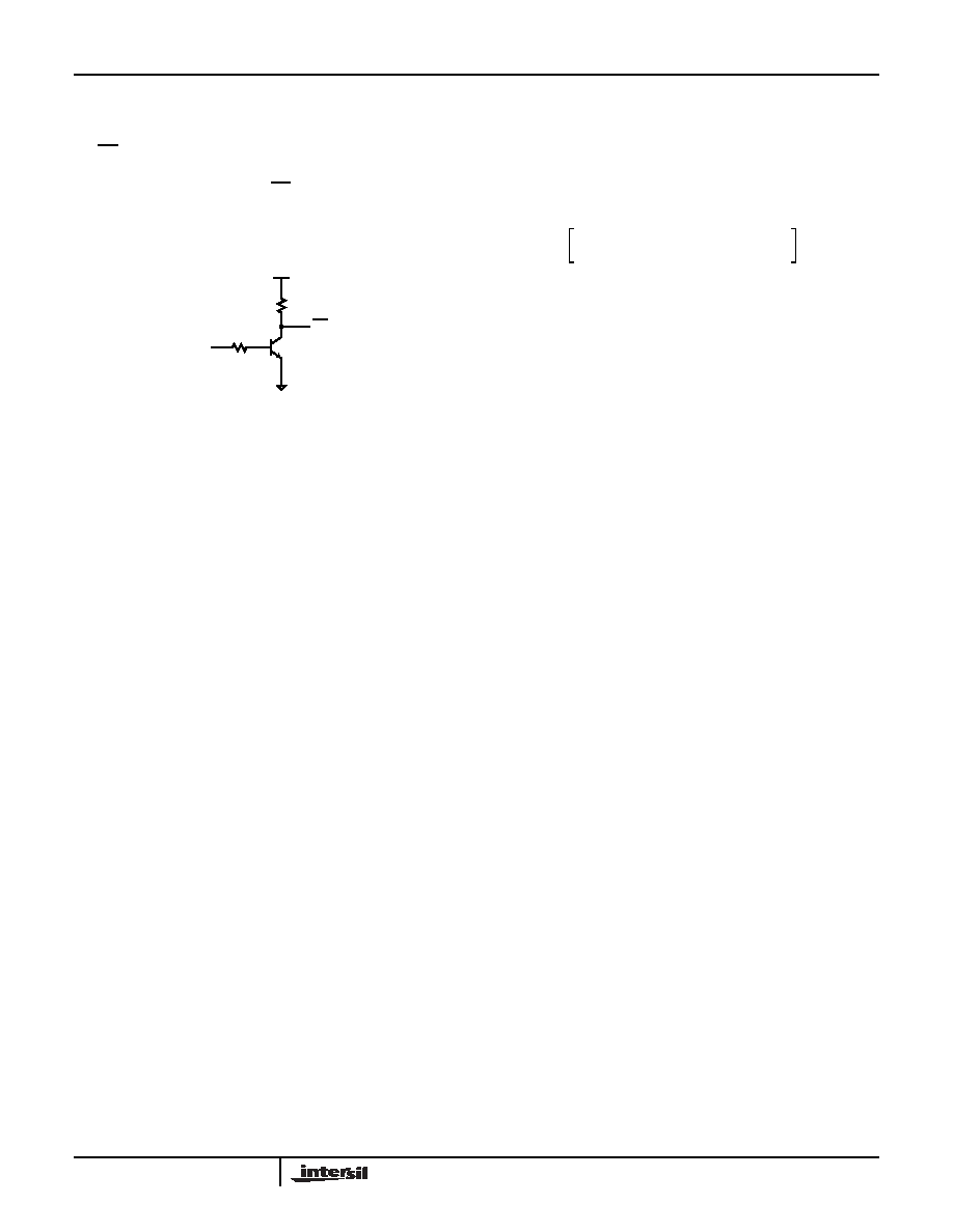
If a TTL signal is used to control the enabled/disabled
function, Figure 26 could be used to convert the TTL signal
to CMOS signal.
Output Drive Capability
The EL5175 and EL5375 have internal short circuit
protection. Its typical short circuit current is ±67mA. If the
output is shorted indefinitely, the power dissipation could
easily increase such that the part will be destroyed.
Maximum reliability is maintained if the output current never
exceeds ±60mA. This limit is set by the design of the internal
metal interconnections.
Power Dissipation
With the high output drive capability of the EL5175 and
EL5375, it is possible to exceed the +135°C absolute
maximum junction temperature under certain load current
conditions. Therefore, it is important to calculate the
maximum junction temperature for the application to
determine if the load conditions or package types need to be
modified for the amplifier to remain in the safe operating
area.
The maximum power dissipation allowed in a package is
determined according to Equation 3:
TJMAX = Maximum junction temperature
TAMAX = Maximum ambient temperature
θJA = Thermal resistance of the package
Assume the REF pin is tired to GND for VS = ±5V
application, the maximum power dissipation actually
produced by an IC is the total quiescent supply current times
the total power supply voltage, plus the power in the IC due
to the load, or:
For sourcing, see Equation 4:
For sinking, see Equation 5:
Where:
VS = Total supply voltage
ISMAX = Maximum quiescent supply current per channel
VOUT = Maximum output voltage of the application
RLOAD = Load resistance
ILOAD = Load current
i = Number of channels
By setting the two PDMAX equations equal to each other, we
can solve the output current and RLOAD to avoid the device
overheat.
Power Supply Bypassing and Printed Circuit
Board Layout
As with any high frequency device, a good printed circuit
board layout is necessary for optimum performance. Lead
lengths should be as short as possible. The power supply
pin must be well bypassed to reduce the risk of oscillation.
For normal single supply operation, where the VS- pin is
connected to the ground plane, a single 4.7F tantalum
capacitor in parallel with a 0.1F ceramic capacitor from VS+
to GND will suffice. This same capacitor combination should
be placed at each supply pin to ground if split supplies are to
be used. In this case, the VS- pin becomes the negative
supply rail.
For good AC performance, parasitic capacitance should be
kept to a minimum. Use of wire-wound resistors should be
avoided because of their additional series inductance. Use
of sockets should also be avoided if possible. Sockets add
parasitic inductance and capacitance that can result in
compromised performance. Minimizing parasitic capacitance
at the amplifier's inverting input pin is very important. The
feedback resistor should be placed very close to the
inverting input pin. Strip line design techniques are
recommended for the signal traces.
1k
10k
5V
EN
CMOS/TTL
FIGURE 26. CONVERSION OF TTL SIGNAL TO CMOS SIGNAL
PDMAX
TJMAX TAMAX
–
Θ
JA
---------------------------------------------
=
(EQ. 3)
PDMAX
VS ISMAX VS+
(
VOUT)
VOUT
RLOAD
--------------------
i
×
–
+
×
=
(EQ. 4)
PDMAX
VS ISMAX VOUT
(
VS-) ILOAD] i
×
–
+
×
[
=
(EQ. 5)
EL5175, EL5375
相关PDF资料 |
PDF描述 |
|---|---|
| MME25-044 | CONN RACK/PANEL 44POS 5A |
| 37204-1BE0-004 PL | CONN SOCKET 4POS 2MM R/A SMD |
| 953414-6602-AR | CONN SOCKET 14POS 2MM VERT T/H |
| 150210-6002-TB | CONN 10POS 2MM SOCKET VERT PC MT |
| MAX367CWN+ | IC SIGNAL-LINE CIRC PROT 18-SOIC |
相关代理商/技术参数 |
参数描述 |
|---|---|
| EL5375IU-T13 | 功能描述:IC AMP TRPL DIFF 550MHZ 24-QSOP RoHS:否 类别:集成电路 (IC) >> Linear - Amplifiers - Instrumentation 系列:- 标准包装:50 系列:LinCMOS™ 放大器类型:通用 电路数:4 输出类型:- 转换速率:0.05 V/µs 增益带宽积:110kHz -3db带宽:- 电流 - 输入偏压:0.7pA 电压 - 输入偏移:210µV 电流 - 电源:57µA 电流 - 输出 / 通道:30mA 电压 - 电源,单路/双路(±):3 V ~ 16 V,±1.5 V ~ 8 V 工作温度:-40°C ~ 85°C 安装类型:表面贴装 封装/外壳:14-SOIC(0.154",3.90mm 宽) 供应商设备封装:14-SOIC 包装:管件 产品目录页面:865 (CN2011-ZH PDF) 其它名称:296-1834296-1834-5 |
| EL5375IU-T7 | 功能描述:IC AMP TRPL DIFF 550MHZ 24-QSOP RoHS:否 类别:集成电路 (IC) >> Linear - Amplifiers - Instrumentation 系列:- 标准包装:1,000 系列:- 放大器类型:电压反馈 电路数:4 输出类型:满摆幅 转换速率:33 V/µs 增益带宽积:20MHz -3db带宽:30MHz 电流 - 输入偏压:2nA 电压 - 输入偏移:3000µV 电流 - 电源:2.5mA 电流 - 输出 / 通道:30mA 电压 - 电源,单路/双路(±):4.5 V ~ 16.5 V,±2.25 V ~ 8.25 V 工作温度:-40°C ~ 85°C 安装类型:表面贴装 封装/外壳:14-SOIC(0.154",3.90mm 宽) 供应商设备封装:14-SOIC 包装:带卷 (TR) |
| EL5375IUZ | 功能描述:差分放大器 EL5375IUZ 500MHZ TRI PLE DIFF LINE REC RoHS:否 制造商:Texas Instruments 通道数量:1 Channel 带宽:2.4 GHz 可用增益调整:6 dB to 26 dB 输入补偿电压: 共模抑制比(最小值):- 40 dB 工作电源电压:4.75 V to 5.25 V 电源电流:100 mA 最大工作温度:+ 85 C 最小工作温度:- 40 C 安装风格:SMD/SMT 封装 / 箱体:WQFN-24 封装:Reel |
| EL5375IUZ-T13 | 功能描述:差分放大器 EL5375IUZ 500 MHZ TPL DIFF LINECVR RoHS:否 制造商:Texas Instruments 通道数量:1 Channel 带宽:2.4 GHz 可用增益调整:6 dB to 26 dB 输入补偿电压: 共模抑制比(最小值):- 40 dB 工作电源电压:4.75 V to 5.25 V 电源电流:100 mA 最大工作温度:+ 85 C 最小工作温度:- 40 C 安装风格:SMD/SMT 封装 / 箱体:WQFN-24 封装:Reel |
| EL5375IUZ-T7 | 功能描述:差分放大器 EL5375IUZ 500 MHZ TPL DIFF LINECVR RoHS:否 制造商:Texas Instruments 通道数量:1 Channel 带宽:2.4 GHz 可用增益调整:6 dB to 26 dB 输入补偿电压: 共模抑制比(最小值):- 40 dB 工作电源电压:4.75 V to 5.25 V 电源电流:100 mA 最大工作温度:+ 85 C 最小工作温度:- 40 C 安装风格:SMD/SMT 封装 / 箱体:WQFN-24 封装:Reel |
发布紧急采购,3分钟左右您将得到回复。