参数资料
| 型号: | EL5420TILZ |
| 厂商: | Intersil |
| 文件页数: | 5/17页 |
| 文件大小: | 0K |
| 描述: | IC OPAMP GP RR 12MHZ QD 16QFN |
| 标准包装: | 90 |
| 放大器类型: | 电压反馈 |
| 电路数: | 4 |
| 输出类型: | 满摆幅 |
| 转换速率: | 12 V/µs |
| 增益带宽积: | 8MHz |
| -3db带宽: | 12MHz |
| 电流 - 输入偏压: | 2nA |
| 电压 - 输入偏移: | 4000µV |
| 电流 - 电源: | 500µA |
| 电流 - 输出 / 通道: | 70mA |
| 电压 - 电源,单路/双路(±): | 4.5 V ~ 19 V,±2.25 V ~ 9.5 V |
| 工作温度: | -40°C ~ 85°C |
| 安装类型: | 表面贴装 |
| 封装/外壳: | 16-VQFN 裸露焊盘 |
| 供应商设备封装: | 16-QFN-EP(4x4) |
| 包装: | 管件 |
13
FN6838.0
September 25, 2009
ON the outputs by putting them in a low impedance (normal)
operating state.
Driving Capacitive Loads
As load capacitance increases, the -3dB bandwidth will
decrease and peaking can occur. Depending on the
application, it may be necessary to reduce peaking and to
improve device stability. To improve device stability a
snubber circuit or a series resistor may be added to the
output of the EL5420T.
A snubber is a shunt load consisting of a resistor in series
with a capacitor. An optimized snubber can improve the
phase margin and the stability of the EL5420T. The
advantage of a snubber circuit is that it does not draw any
DC load current or reduce the gain.
Another method to reduce peaking is to add a series output
resistor (typically between 1
Ω to 10Ω). Depending on the
capacitive loading, a small value resistor may be the most
appropriate choice to minimize any reduction in gain.
Power Dissipation
With the high-output drive capability of the EL5420T
amplifiers, it is possible to exceed the +150°C absolute
maximum junction temperature under certain load current
conditions. It is important to calculate the maximum power
dissipation of the EL5420T in the application. Proper load
conditions will ensure that the EL5420T junction temperature
stays within a safe operating region.
The maximum power dissipation allowed in a package is
determined according to Equation 1:
where:
TJMAX = Maximum junction temperature
TAMAX = Maximum ambient temperature
ΘJA = Thermal resistance of the package
PDMAX = Maximum power dissipation allowed
The total power dissipation produced by an IC is the total
quiescent supply current times the total power supply
voltage, plus the power dissipation in the IC due to the loads,
or:
when sourcing, and:
when sinking,
where:
i = 1 to 4
(1, 2, 3, 4 corresponds to Channel A, B, C, D respectively)
VS = Total supply voltage (VS+ - VS-)
VS+ = Positive supply voltage
VS- = Negative supply voltage
ISMAX = Maximum supply current per amplifier
(ISMAX = EL5420T quiescent current ÷ 4)
VOUT = Output voltage
ILOAD = Load current
Device overheating can be avoided by calculating the
minimum resistive load condition, RLOAD, resulting in the
highest power dissipation. To find RLOAD set the two PDMAX
equations equal to each other and solve for VOUT/ILOAD.
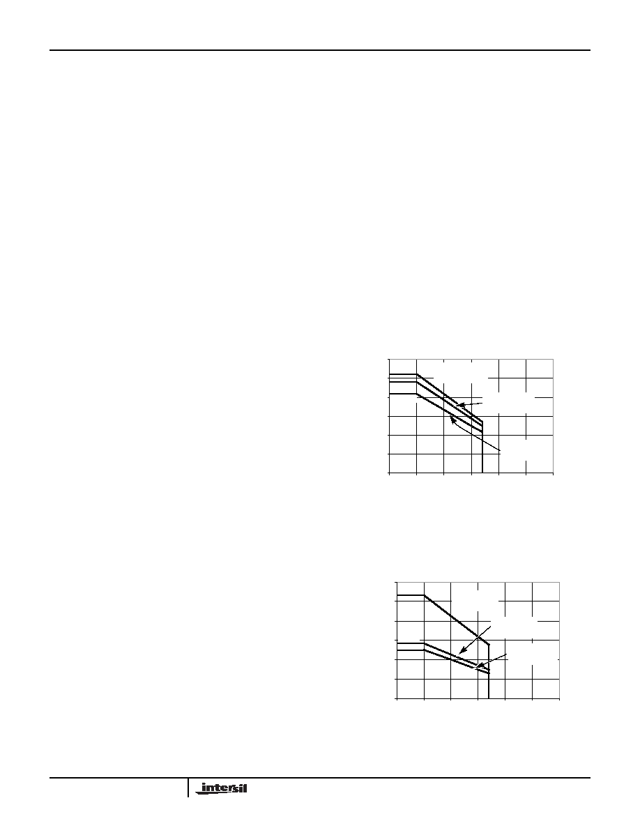
Reference the package power dissipation curves, Figures 30
and 31, for further information.
P
DMAX
T
JMAX
T
AMAX
–
θ
JA
---------------------------------------------
=
(EQ. 1)
P
DMAX
ΣiV
[
S
I
SMAX
V
(
S+VOUTi )
I
LOAD i
×
–
+
×]
=
(EQ. 2)
P
DMAX
ΣiV
[
S
I
SMAX
V
(
OUTiVS- )
I
LOADi
×
–
+
×]
=
(EQ. 3)
0.0
0.2
0.4
0.6
0.8
1.0
1.2
0
25
50
75
100
125
150
Am bient Te mpera ture (°C)
P
o
w
e
rD
is
s
ip
a
ti
on
(
W
)
FIGURE 30. PACKAGE POWER DISSIPATION vs AMBIENT
TEMPERATURE
JEDEC JESD51-3 LOW EFFECTIVE THERMAL
CONDUCTIVITY TEST BOARD
1.04W
962mW
833mW
θJA = 120°C/W
SOIC14
θJA = 150°C/W
TSSOP14
θJA = 130°C/W
QFN16
85
FIGURE 31. PACKAGE POWER DISSIPATION vs AMBIENT
TEMPERATURE
JEDEC JESD51-7 HIGH EFFECTIVE THERMAL
0.0
0.5
1.0
1.5
2.0
2.5
3.0
0
25
50
75
100
125
150
A m b ien t T e m p e ratu re (°C )
P
o
wer
D
iss
ip
at
io
n
(
W
)
2.66W
1.42W
1.25W
θJA = 47°C/W
QFN16
θJA = 100°C/W
TSSOP14
θJA = 88°C/W
SOIC14
85
EL5420T
相关PDF资料 |
PDF描述 |
|---|---|
| 951232-4620-AR-PT | CONN HEADER 32POS 2MM R/A SMD |
| 208457096013025 | CONNECTOR RECEPT 96POS R/A |
| M80-8271842 | CONN HDR 2MM SMT W/LATCH 18POS |
| 961234-5500-AR-PR | CONN HEADER R/A 34POS GOLD SMD |
| 228458096001037 | CONNECTOR RECEPT 96POS PRESS |
相关代理商/技术参数 |
参数描述 |
|---|---|
| EL5420TILZ-T13 | 功能描述:运算放大器 - 运放 EL5420TILZ 12 MHZ QD R2R I/O OP RoHS:否 制造商:STMicroelectronics 通道数量:4 共模抑制比(最小值):63 dB 输入补偿电压:1 mV 输入偏流(最大值):10 pA 工作电源电压:2.7 V to 5.5 V 安装风格:SMD/SMT 封装 / 箱体:QFN-16 转换速度:0.89 V/us 关闭:No 输出电流:55 mA 最大工作温度:+ 125 C 封装:Reel |
| EL5420TILZ-T7 | 功能描述:运算放大器 - 运放 EL5420TILZ 12 MHZ QD R2R I/O OP RoHS:否 制造商:STMicroelectronics 通道数量:4 共模抑制比(最小值):63 dB 输入补偿电压:1 mV 输入偏流(最大值):10 pA 工作电源电压:2.7 V to 5.5 V 安装风格:SMD/SMT 封装 / 箱体:QFN-16 转换速度:0.89 V/us 关闭:No 输出电流:55 mA 最大工作温度:+ 125 C 封装:Reel |
| EL5420TIRZ | 功能描述:运算放大器 - 运放 EL5420TIRZ 12 MHZ QD R2R I/O OP RoHS:否 制造商:STMicroelectronics 通道数量:4 共模抑制比(最小值):63 dB 输入补偿电压:1 mV 输入偏流(最大值):10 pA 工作电源电压:2.7 V to 5.5 V 安装风格:SMD/SMT 封装 / 箱体:QFN-16 转换速度:0.89 V/us 关闭:No 输出电流:55 mA 最大工作温度:+ 125 C 封装:Reel |
| EL5420TIRZ-T13 | 功能描述:运算放大器 - 运放 EL5420TIRZ 12 MHZ QD R2R I/O OP RoHS:否 制造商:STMicroelectronics 通道数量:4 共模抑制比(最小值):63 dB 输入补偿电压:1 mV 输入偏流(最大值):10 pA 工作电源电压:2.7 V to 5.5 V 安装风格:SMD/SMT 封装 / 箱体:QFN-16 转换速度:0.89 V/us 关闭:No 输出电流:55 mA 最大工作温度:+ 125 C 封装:Reel |
| EL5420TIRZ-T7 | 功能描述:运算放大器 - 运放 EL5420TIRZ 12 MHZ QD R2R I/O OP RoHS:否 制造商:STMicroelectronics 通道数量:4 共模抑制比(最小值):63 dB 输入补偿电压:1 mV 输入偏流(最大值):10 pA 工作电源电压:2.7 V to 5.5 V 安装风格:SMD/SMT 封装 / 箱体:QFN-16 转换速度:0.89 V/us 关闭:No 输出电流:55 mA 最大工作温度:+ 125 C 封装:Reel |
发布紧急采购,3分钟左右您将得到回复。