参数资料
| 型号: | EL5423CLZ |
| 厂商: | Intersil |
| 文件页数: | 4/17页 |
| 文件大小: | 0K |
| 描述: | IC BUFFER I/O 12MHZ 12CH 32-QFN |
| 标准包装: | 60 |
| 放大器类型: | 缓冲器 |
| 电路数: | 12 |
| 输出类型: | 满摆幅 |
| 转换速率: | 18 V/µs |
| -3db带宽: | 12MHz |
| 电流 - 输入偏压: | 2nA |
| 电压 - 输入偏移: | 500µV |
| 电流 - 电源: | 7.8mA |
| 电流 - 输出 / 通道: | 200mA |
| 电压 - 电源,单路/双路(±): | 4.5 V ~ 16.5 V,±2.25 V ~ 8.25 V |
| 工作温度: | -40°C ~ 85°C |
| 安装类型: | 表面贴装 |
| 封装/外壳: | 32-VFQFN 裸露焊盘 |
| 供应商设备封装: | 32-QFN-EP |
| 包装: | 管件 |
| 产品目录页面: | 1233 (CN2011-ZH PDF) |
12
FN7176.3
August 31, 2010
Applications Information
Product Description
The EL5123, EL5223, EL5323, and EL5423 unity gain
buffers are fabricated using a high voltage CMOS process. It
exhibits rail-to-rail input and output capability and has low
power consumption (600A per buffer). These features
make the EL5123, EL5223, EL5323, and EL5423 ideal for a
wide range of general-purpose applications. When driving a
load of 10k
Ω and 12pF, the EL5123, EL5223, EL5323, and
EL5423 have a -3dB bandwidth of 12MHz and exhibits
15V/s slew rate.
Operating Voltage, Input, and Output
The EL5123, EL5223, EL5323, and EL5423 are specified
with a single nominal supply voltage from 5V to 15V or a split
supply with its total range from 5V to 15V. Correct operation
is guaranteed for a supply range of 4.5V to 16.5V. Most
EL5123, EL5223, EL5323, and EL5423 specifications are
stable over both the full supply range and operating
temperatures of -40°C to +85°C. Parameter variations with
operating voltage and/or temperature are shown in the
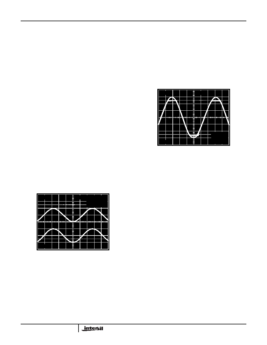
The output swings of the EL5123, EL5223, EL5323, and
EL5423 typically extend to within 50mV of positive and
negative supply rails with load currents of 5mA. Decreasing
load currents will extend the output voltage range even closer
to the supply rails. Figure 24 shows the input and output
waveforms for the device. Operation is from ±5V supply with a
10k
Ω load connected to GND. The input is a 10VP-P sinusoid.
The output voltage is approximately 9.985VP-P.
FIGURE 24. OPERATION WITH RAIL-TO-RAIL INPUT AND
OUTPUT
Short Circuit Current Limit
The EL5123, EL5223, EL5323, and EL5423 will limit the
short circuit current to ±120mA if the output is directly
shorted to the positive or the negative supply. If an output is
shorted indefinitely, the power dissipation could easily
increase such that the device may be damaged. Maximum
reliability is maintained if the output continuous current never
exceeds ±30mA. This limit is set by the design of the internal
metal interconnects.
Output Phase Reversal
The EL5123, EL5223, EL5323, and EL5423 are immune to
phase reversal as long as the input voltage is limited from
output of the device with the input voltage driven beyond the
supply rails. Although the device's output will not change
phase, the input's over-voltage should be avoided. If an input
voltage exceeds supply voltage by more than 0.6V,
electrostatic protection diodes placed in the input stage of
the device begin to conduct and overvoltage damage could
occur.
FIGURE 25. OPERATION WITH BEYOND-THE-RAILS INPUT
Power Dissipation
With the high-output drive capability of the EL5123, EL5223,
EL5323, and EL5423 buffer, it is possible to exceed the
+125°C “absolute-maximum junction temperature” under
certain load current conditions. Therefore, it is important to
calculate the maximum junction temperature for the
application to determine if load conditions need to be
modified for the buffer to remain in the safe operating area.
The maximum power dissipation allowed in a package is
determined according to Equation 1:
where:
TJMAX = Maximum junction temperature
TAMAX = Maximum ambient temperature
θJA = Thermal resistance of the package
PDMAX = Maximum power dissipation in the package
The maximum power dissipation actually produced by an IC
is the total quiescent supply current times the total power
supply voltage, plus the power in the IC due to the loads, or:
OUT
P
UT
INP
U
T
5V
10s
VS = ±5V
TA = +25°C
VIN = 10VP-P
1V
10s
VS=±2.5V
TA=25°C
VIN=6VP-P
PDMAX
TJMAX TAMAX
–
Θ
d JA
---------------------------------------------
=
(EQ. 1)
PDMAX
ΣiV
[
S
ISMAX VS+
(
VOUTi) ILOADi]
×
–
+
×
=
(EQ. 2)
EL5123, EL5223, EL5323, EL5423
相关PDF资料 |
PDF描述 |
|---|---|
| EL5424ILZ-T7 | IC BUFFER LP 12CH 12MHZ 32-QFN |
| EL5427CRZ-T7 | IC BUFFER LP 12CH 2.5MHZ 28TSSOP |
| EL5444CUZ-T7 | IC AMP VFA QUAD 100MHZ 16-QSOP |
| EL5451ISZ-T13 | IC VFA QUAD 200MHZ 14-SOIC |
| EL5462ISZ | IC AMP LOW PWR 500MHZ 14-SOIC |
相关代理商/技术参数 |
参数描述 |
|---|---|
| EL5423CLZ-T13 | 功能描述:运算放大器 - 运放 EL5423CLZ 12MHZ 12 CH BUFR RoHS:否 制造商:STMicroelectronics 通道数量:4 共模抑制比(最小值):63 dB 输入补偿电压:1 mV 输入偏流(最大值):10 pA 工作电源电压:2.7 V to 5.5 V 安装风格:SMD/SMT 封装 / 箱体:QFN-16 转换速度:0.89 V/us 关闭:No 输出电流:55 mA 最大工作温度:+ 125 C 封装:Reel |
| EL5423CLZ-T7 | 功能描述:运算放大器 - 运放 EL5423CLZ 12MHZ 12 CH BUFR RoHS:否 制造商:STMicroelectronics 通道数量:4 共模抑制比(最小值):63 dB 输入补偿电压:1 mV 输入偏流(最大值):10 pA 工作电源电压:2.7 V to 5.5 V 安装风格:SMD/SMT 封装 / 箱体:QFN-16 转换速度:0.89 V/us 关闭:No 输出电流:55 mA 最大工作温度:+ 125 C 封装:Reel |
| EL5423CR | 功能描述:IC OPAMP R-R 12CH 12MHZ 28-TSSOP RoHS:否 类别:集成电路 (IC) >> Linear - Amplifiers - Instrumentation 系列:- 标准包装:50 系列:LinCMOS™ 放大器类型:通用 电路数:4 输出类型:- 转换速率:0.05 V/µs 增益带宽积:110kHz -3db带宽:- 电流 - 输入偏压:0.7pA 电压 - 输入偏移:210µV 电流 - 电源:57µA 电流 - 输出 / 通道:30mA 电压 - 电源,单路/双路(±):3 V ~ 16 V,±1.5 V ~ 8 V 工作温度:-40°C ~ 85°C 安装类型:表面贴装 封装/外壳:14-SOIC(0.154",3.90mm 宽) 供应商设备封装:14-SOIC 包装:管件 产品目录页面:865 (CN2011-ZH PDF) 其它名称:296-1834296-1834-5 |
| EL5423CR-T13 | 功能描述:IC OPAMP R-R 12CH 12MHZ 28-TSSOP RoHS:否 类别:集成电路 (IC) >> Linear - Amplifiers - Instrumentation 系列:- 标准包装:50 系列:LinCMOS™ 放大器类型:通用 电路数:4 输出类型:- 转换速率:0.05 V/µs 增益带宽积:110kHz -3db带宽:- 电流 - 输入偏压:0.7pA 电压 - 输入偏移:210µV 电流 - 电源:57µA 电流 - 输出 / 通道:30mA 电压 - 电源,单路/双路(±):3 V ~ 16 V,±1.5 V ~ 8 V 工作温度:-40°C ~ 85°C 安装类型:表面贴装 封装/外壳:14-SOIC(0.154",3.90mm 宽) 供应商设备封装:14-SOIC 包装:管件 产品目录页面:865 (CN2011-ZH PDF) 其它名称:296-1834296-1834-5 |
| EL5423CR-T7 | 功能描述:IC OPAMP R-R 12CH 12MHZ 28-TSSOP RoHS:否 类别:集成电路 (IC) >> Linear - Amplifiers - Instrumentation 系列:- 标准包装:50 系列:LinCMOS™ 放大器类型:通用 电路数:4 输出类型:- 转换速率:0.05 V/µs 增益带宽积:110kHz -3db带宽:- 电流 - 输入偏压:0.7pA 电压 - 输入偏移:210µV 电流 - 电源:57µA 电流 - 输出 / 通道:30mA 电压 - 电源,单路/双路(±):3 V ~ 16 V,±1.5 V ~ 8 V 工作温度:-40°C ~ 85°C 安装类型:表面贴装 封装/外壳:14-SOIC(0.154",3.90mm 宽) 供应商设备封装:14-SOIC 包装:管件 产品目录页面:865 (CN2011-ZH PDF) 其它名称:296-1834296-1834-5 |
发布紧急采购,3分钟左右您将得到回复。