参数资料
| 型号: | EL5524IREZ-T7 |
| 厂商: | Intersil |
| 文件页数: | 11/11页 |
| 文件大小: | 0K |
| 描述: | IC BUFFER 4XGAMMA 5.4MA 14HTSSOP |
| 标准包装: | 1,000 |
| 应用: | TFT-LCD 面板:伽玛缓冲器,VCOM 驱动器 |
| 输出类型: | 满摆幅 |
| 电路数: | 4 |
| -3db带宽: | 12MHz |
| 转换速率: | 15 V/µs |
| 电流 - 电源: | 5.4mA |
| 电流 - 输出 / 通道: | 140mA |
| 电压 - 电源,单路/双路(±): | 4.5 V ~ 16.5 V,±2.25 V ~ 8.25 V |
| 安装类型: | 表面贴装 |
| 封装/外壳: | 14-TSSOP (0.173",4.40mm 宽)裸露焊盘 |
| 供应商设备封装: | 14-TSSOP-EP |
| 包装: | 带卷 (TR) |
9
Description of Operation and Application
Information
Product Description
The EL5524, EL5624, EL5724, and EL5824 are fabricated
using a high voltage CMOS process. They exhibit rail to rail
input and output capability and have very low power
consumption. When driving a load of 10K and 12pF, the
buffers have a -3dB bandwidth of 12MHz and exhibit 18V/s
slew rate. The VCOM amplifier has a -3dB bandwidth of
35MHz and exhibit 80V/s slew rate.
Input, Output, and Supply Voltage Range
The EL5524, EL5624, EL5724, and EL5824 are specified
with a single nominal supply voltage from 5V to 15V or a split
supply with its total range from 5V to 15V. Correct operation
is guaranteed for a supply range from 4.5V to 16.5V.
The input common-mode voltage range of the EL5524,
EL5624, EL5724, and EL5824 extends 500mV beyond the
supply rails. The output swings of the buffers and VCOM
amplifier typically extend to within 100mV of the positive and
negative supply rails with load currents of 5mA. Decreasing
load currents will extend the output voltage even closer to
each supply rails.
Output Phase Reversal
The EL5524, EL5624, EL5724, and EL5824 are immune to
phase reversal as long as the input voltage is limited from
VS- -0.5V to VS+ +0.5V. Although the device's output will not
change phase, the input's overvoltage should be avoided. If
an input voltage exceeds supply voltage by more than 0.6V,
electrostatic protection diode placed in the input stage of the
device begin to conduct and overvoltage damage could
occur.
Choice of Feedback Resistor and Gain Bandwidth
Product for VCOM Amplifier
For applications that require a gain of +1, no feedback
resistor is required. Just short the output pin to the inverting
input pin. For gains greater than +1, the feedback resistor
forms a pole with the parasitic capacitance at the inverting
input. As this pole becomes smaller, the amplifier's phase
margin is reduced. This causes ringing in the time domain
and peaking in the frequency domain. Therefore, RF has
some maximum value that should not be exceeded for
optimum performance. If a large value of RF must be used, a
small capacitor in the few Pico farad range in parallel with RF
can help to reduce the ringing and peaking at the expense of
reducing the bandwidth.
As far as the output stage of the amplifier is concerned, the
output stage is also a gain stage with the load. RF and RG
appear in parallel with RL for gains other than +1. As this
combination gets smaller, the bandwidth falls off.
Consequently, RF also has a minimum value that should not
be exceeded for optimum performance. For gain of +1, RF =
0 is optimum. For the gains other than +1, optimum
response is obtained with RF between 1k to 5k.
The VCOM amplifier has a gain bandwidth product of
20MHz. For gains
≥5, its bandwidth can be predicted by the
following equation:
Output Drive Capability
The EL5524, EL5624, EL5724, and EL5824 do not have
internal short-circuit protection circuitry. The buffers will limit
the short circuit current to ±120mA and the VCOM amplifier
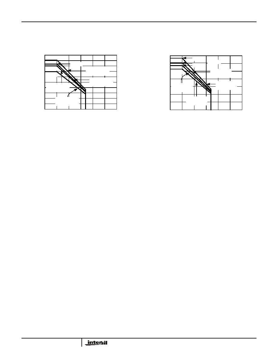
FIGURE 19. PACKAGE POWER DISSIPATION vs AMBIENT
TEMPERATURE
FIGURE 20. PACKAGE POWER DISSIPATION vs AMBIENT
TEMPERATURE
Typical Performance Curves (Continued)
JEDEC JESD51-3 LOW EFFECTIVE THERMAL
CONDUCTIVITY TEST BOARD
1
0.9
0.6
0.4
0.3
0.2
0.1
0
255075
100
150
AMBIENT TEMPERATURE (°C)
POWER
DISS
IP
A
T
ION
(W)
85
0.8
0.5
0.7
125
909mW
800mW
694mW
833mW
θJA=110°C/W
HTSSOP28
θJA=120°C/W
HTSSOP24
θJA=125°C/W
HTSSOP20
θJA=144°C/W
HTSSOP14
JEDEC JESD51-7 HIGH EFFECTIVE THERMAL
CONDUCTIVITY TEST BOARD -
HTSSOP EXPOSED DIEPAD SOLDERED TO
PCB PER JESD51-5
3.5
3
2.5
1.5
1
0.5
0
255075
100
150
AMBIENT TEMPERATURE (°C)
P
O
WER
DIS
S
IP
A
T
ION
(W
)
125
85
2
2.632W
3.333W
3.030W
2.857W
θJA=35°C/W
HTSSOP20
θJA=38°C/W
HTSSOP14
θJA=30°C/W
HTSSOP28
θJA=33°C/W
HTSSOP24
Gain
BW
20MHz
=
×
EL5524, EL5624, EL5724, EL5824
相关PDF资料 |
PDF描述 |
|---|---|
| EL5524IREZ-T13 | IC BUFFER 4XGAMMA 5.4MA 14HTSSOP |
| ISL59421IUZ-T7 | IC AMP MULTIPLEX 865MHZ 10-MSOP |
| ISL59421IUZ-T13 | IC AMP MULTIPLEX 865MHZ 10-MSOP |
| MAX5548ETE+ | IC DAC 8BIT DUAL 30MA 16-TQFN |
| ISL59420IUZ-T13 | IC AMP MULTIPLEX 400MHZ 10-MSOP |
相关代理商/技术参数 |
参数描述 |
|---|---|
| EL5525 | 制造商:INTERSIL 制造商全称:Intersil Corporation 功能描述:18-Channel TFT-LCD Reference Voltage Generator |
| EL552-5 | 制造商:未知厂家 制造商全称:未知厂家 功能描述:Logic IC |
| EL5525 WAF | 制造商:Intersil Corporation 功能描述: |
| EL552-5.5 | 制造商:未知厂家 制造商全称:未知厂家 功能描述:Logic IC |
| EL5525IRE | 功能描述:IC VREF GEN 18CH TFTLCD 38HTSSOP RoHS:否 类别:集成电路 (IC) >> PMIC - 稳压器 - 专用型 系列:- 产品培训模块:Lead (SnPb) Finish for COTS Obsolescence Mitigation Program 标准包装:2,000 系列:- 应用:电源,ICERA E400,E450 输入电压:4.1 V ~ 5.5 V 输出数:10 输出电压:可编程 工作温度:-40°C ~ 85°C 安装类型:表面贴装 封装/外壳:42-WFBGA,WLCSP 供应商设备封装:42-WLP 包装:带卷 (TR) |
发布紧急采购,3分钟左右您将得到回复。