参数资料
| 型号: | EL7520AILZ-T7 |
| 厂商: | Intersil |
| 文件页数: | 12/18页 |
| 文件大小: | 0K |
| 描述: | IC CTRLR DC/DC 4-CHAN 20-QFN |
| 标准包装: | 1,000 |
| 应用: | 控制器,TFT LCD |
| 输入电压: | 3 V ~ 5.5 V |
| 输出数: | 4 |
| 工作温度: | -40°C ~ 85°C |
| 安装类型: | 表面贴装 |
| 封装/外壳: | 20-VFQFN 裸露焊盘 |
| 供应商设备封装: | 20-QFN 裸露焊盘(4x4) |
| 包装: | 带卷 (TR) |
�� �
�
�EL7520,� EL7520A�
�I� LAVG� =� -------------�
�Input� Capacitor�
�The� input� capacitor� is� used� to� supply� the� current� to� the�
�converter.� It� is� recommended� that� C� IN� be� larger� than� 10μF.�
�The� reflected� ripple� voltage� will� be� smaller� with� larger� C� IN� .�
�The� voltage� rating� of� input� capacitor� should� be� larger� than�
�maximum� input� voltage.�
�Boost� Inductor�
�A� 3.3μH� inductor� is� recommended� due� to� the� fixed� internal�
�slope� compensation.� The� inductor� must� be� able� to� handle�
�the� following� average� and� peak� current:�
�I� O�
�1� –� D�
�2�
�?� I� L�
�I� LPK� =� I� LAVG� +� --------�
�Switching� MOSFET�
�Due� to� the� parasitic� inductance� of� the� trace,� the� MOSFET�
�will� experience� spikes� higher� that� the� output� voltage� when�
�the� MOSFET� turns� off.� Thus,� a� MOSFET� with� enough�
�voltage� margin� is� needed.�
�The� R� DS(ON)� of� the� MOSFET� is� critical� for� power� dissipation�
�and� current� limit.� A� MOSFET� with� low� R� DS(ON)� is� desired� to�
�get� high� efficiency� and� output� current,� but� very� low� R� DS(ON)�
�will� reduce� the� loop� stability.� A� MOSFET� with� 20m� ?� to� 50m� ?�
�R� DS(ON)� is� recommended.� Some� recommended� MOSFETs�
�are� shown� in� following� table.�
�For� low� ESR� ceramic� capacitors,� the� output� ripple� is�
�dominated� by� the� charging� and� discharging� of� the� output�
�capacitor.� The� voltage� rating� of� the� output� capacitor� should�
�be� greater� than� the� maximum� output� voltage.�
�Compensation�
�The� EL7520� and� EL7520A� can� operate� in� either� P� mode� or�
�PI� mode.� Connecting� C� INT� pin� directly� to� V� IN� will� enable�
�P� mode.� For� better� load� regulation,� use� PI� mode� with� a�
�2.2nF� capacitor� between� C� INT� and� ground.�
�Linear-Regulator� Controllers� (V� ON� ,� V� LOGIC� ,� and�
�V� OFF� )�
�The� EL7520,� EL7520A� include� three� independent� linear-�
�regulator� controllers,� in� which� two� are� positive� output� voltage�
�(V� ON� and� V� LOGIC� ),� and� one� is� negative.� The� V� ON� ,� V� OFF� ,�
�and� V� LOGIC� linear-regulator� controller� functional� diagrams,�
�applications� circuits� are� shown� in� Figures� 27,� 28,� and� 29�
�respectively.�
�Calculation� of� the� Linear� Regulator� Base-Emitter�
�Resistors� (R� BL� ,� R� BP� and� R� BN� )�
�For� the� pass� transistor� of� the� linear� regulator,� low� frequency�
�gain� (Hfe)� and� unity� gain� freq.� (f� T� )� are� usually� specified� in� the�
�datasheet.� The� pass� transistor� adds� a� pole� to� the� loop� transfer�
�function� at� f� p� =� f� T� /Hfe.� Therefore,� in� order� to� maintain� phase�
�margin� at� low� frequency,� the� best� choice� for� a� pass� device� is�
�often� a� high� frequency� low� gain� switching� transistor.� Further�
�improvement� can� be� obtained� by� adding� a� base-emitter� resistor�
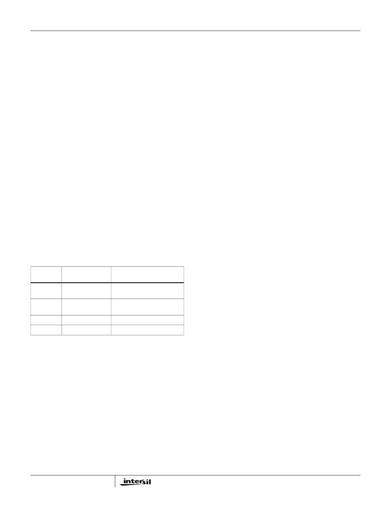
�PART�
�NUMBER�
�FDC655AN�
�TABLE� 2.� RECOMMENDED� MOSFETs�
�MANUFACTURER� FEATURE�
�Fairchild� 6.3A,� 30V,� R� DS(ON)� =� 23m� ?�
�Semiconductor�
�R� BE� (R� BP� ,� R� BL� ,� R� BN� in� the� Functional� Block� Diagram),� which�
�increase� the� pole� frequency� to:� f� p� =� f� T� *(1+� Hfe� *re/R� BE� )/Hfe,�
�where� re� =� KT/qIc.� So� choose� the� lowest� value� R� BE� in� the�
�design� as� long� as� there� is� still� enough� base� current� (I� B� )� to�
�support� the� maximum� output� current� (I� C� ).�
�FDS4488�
�Si7844DP�
�SI6928DQ�
�Fairchild�
�Semiconductor�
�Vishay�
�Vishay�
�7.9A,� 30V,� R� DS(ON)� =� 22m� ?�
�10A,� 30V,� R� DS(ON)� =� 22m� ?�
�20A,� 30V,� R� DS(ON)� =� 30m� ?�
�We� will� take� as� an� example� the� V� LOGIC� linear� regulator.� If� a�
�Fairchild� FMMT549� PNP� transistor� is� used� as� the� external�
�pass� transistor,� Q31� in� the� application� diagram,� then� for� a�
�maximum� V� LOGIC� operating� requirement� of� 500mA� the� data�
�sheet� indicates� Hfe_min� =� 100.�
�V� RIPPLE� =� I� LPK� � ESR� +� ------------------------� � ----------------� � -----�
�V� C� f�
�Rectifier� Diode�
�A� high-speed� diode� is� desired� due� to� the� high� switching�
�frequency.� Schottky� diodes� are� recommended� because� of�
�their� fast� recovery� time� and� low� forward� voltage.� The� rectifier�
�diode� must� meet� the� output� current� and� peak� inductor�
�current� requirements.�
�Output� Capacitor�
�The� output� capacitor� supplies� the� load� directly� and� reduces� the�
�ripple� voltage� at� the� output.� Output� ripple� voltage� consists� of�
�two� components:� the� voltage� drop� due� to� the� inductor� ripple�
�current� flowing� through� the� ESR� of� output� capacitor,� and� the�
�charging� and� discharging� of� the� output� capacitor.�
�V� O� –� V� IN� I� O� 1�
�O� OUT� S�
�12�
�The� base-emitter� saturation� voltage� is:� Vbe_max� =� 1.25V� (note�
�this� is� normally� a� Vbe� ~� 0.7V,� however,� for� the� Q5� transistor� an�
�internal� Darlington� arrangement� is� used� to� increase� it's� current�
�gain,� giving� a� 'base-emitter'� voltage� of� 2� x� V� BE� ).�
�(Note� that� using� a� high� current� Darlington� PNP� transistor� for�
�Q5� requires� that� V� IN� >� V� LOGIC� +� 2V.� Should� a� lower� input�
�voltage� be� required,� then� an� ordinary� high� gain� PNP�
�transistor� should� be� selected� for� Q5� so� as� to� allow� a� lower�
�collector-emitter� saturation� voltage).�
�For� the� EL7520,� EL7520A,� the� minimum� drive� current� is:�
�I_DRVL_min� =� 8mA�
�FN7318.0�
�July� 12,� 2005�
�相关PDF资料 |
PDF描述 |
|---|---|
| EL7520AILZ-T13 | IC CTRLR DC/DC 4-CHAN 20-QFN |
| GMC31DRXS-S734 | CONN EDGECARD 62POS DIP .100 SLD |
| ISL6556BCRZA-T | IC CTRLR MULTIPHASE VRM10 32-QFN |
| ISL6556BCRZ-T | IC CTRLR MULTIPHASE VRM10 32-QFN |
| ESC35DRTI-S734 | CONN EDGECARD 70POS DIP .100 SLD |
相关代理商/技术参数 |
参数描述 |
|---|---|
| EL7520ILZ | 功能描述:电流型 PWM 控制器 EL7520ILZ 4-CH DC-DC CNTRLR RoHS:否 制造商:Texas Instruments 开关频率:27 KHz 上升时间: 下降时间: 工作电源电压:6 V to 15 V 工作电源电流:1.5 mA 输出端数量:1 最大工作温度:+ 105 C 安装风格:SMD/SMT 封装 / 箱体:TSSOP-14 |
| EL7520ILZ-T13 | 功能描述:电流型 PWM 控制器 EL7520ILZ 4-CH DC-DC CNTRLR RoHS:否 制造商:Texas Instruments 开关频率:27 KHz 上升时间: 下降时间: 工作电源电压:6 V to 15 V 工作电源电流:1.5 mA 输出端数量:1 最大工作温度:+ 105 C 安装风格:SMD/SMT 封装 / 箱体:TSSOP-14 |
| EL7520ILZ-T7 | 功能描述:电流型 PWM 控制器 EL7520ILZ 4-CH DC-DC CNTRLR RoHS:否 制造商:Texas Instruments 开关频率:27 KHz 上升时间: 下降时间: 工作电源电压:6 V to 15 V 工作电源电流:1.5 mA 输出端数量:1 最大工作温度:+ 105 C 安装风格:SMD/SMT 封装 / 箱体:TSSOP-14 |
| EL7530 | 制造商:INTERSIL 制造商全称:Intersil Corporation 功能描述:Monolithic 600mA Step-Down Regulator with Low Quiescent Current |
| EL7530_06 | 制造商:INTERSIL 制造商全称:Intersil Corporation 功能描述:Monolithic 600mA Step-Down Regulator with Low Quiescent Current |
发布紧急采购,3分钟左右您将得到回复。