参数资料
| 型号: | EL7584IRZ-T7 |
| 厂商: | Intersil |
| 文件页数: | 13/16页 |
| 文件大小: | 0K |
| 描述: | IC CONV DC/DC 4-CHAN 24-TSSOP |
| 标准包装: | 1,000 |
| 应用: | 转换器,TFT,LCD |
| 输入电压: | 2 V ~ 14 V |
| 输出数: | 2 |
| 输出电压: | 5 V ~ 17 V |
| 工作温度: | -40°C ~ 85°C |
| 安装类型: | 表面贴装 |
| 封装/外壳: | 24-TSSOP(0.173",4.40mm 宽) |
| 供应商设备封装: | 24-TSSOP |
| 包装: | 带卷 (TR) |
�� �
�
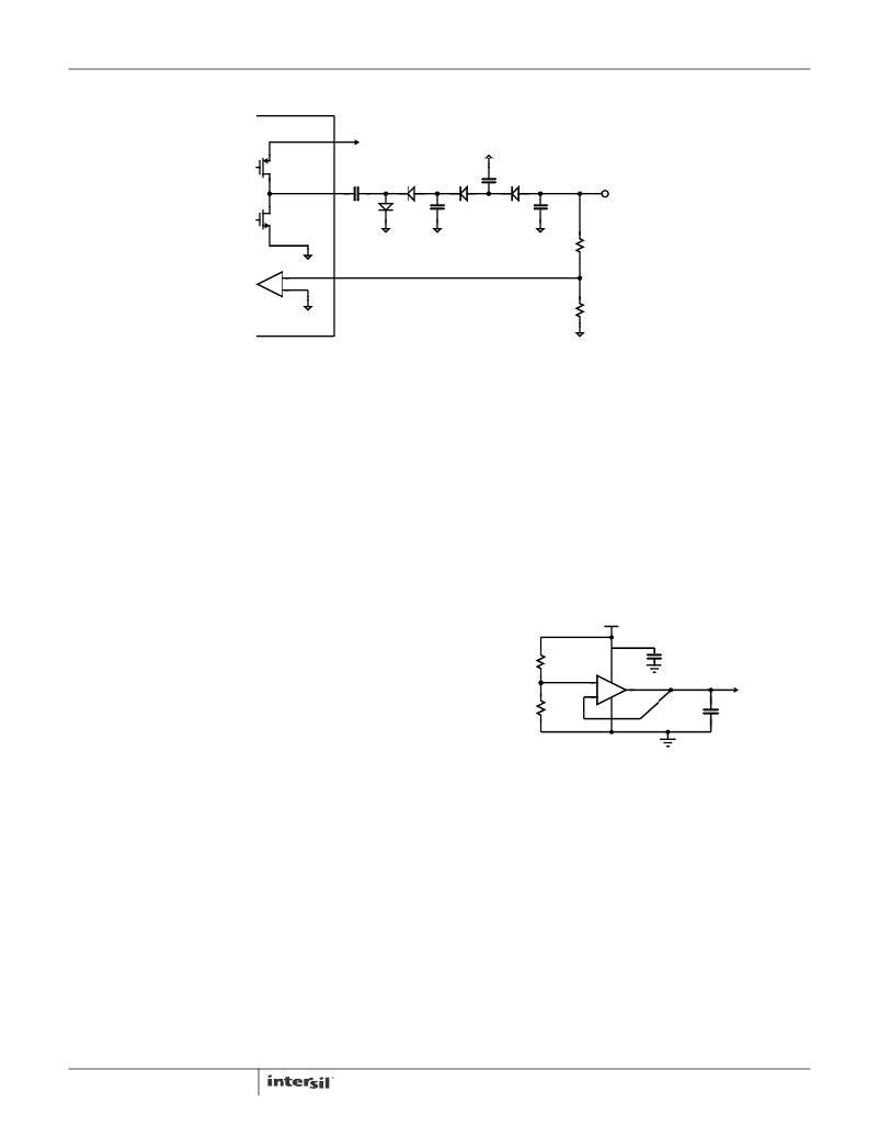
�EL7584�
�Two-Stage� Negative� Charge� Pump� Circuit�
�V� DDN�
�R� ONP�
�5V-17V�
�V� LX�
�C� CPN�
�DRVN�
�R� ONN�
�C� CPN�
�C� OUT2�
�C� OUT2�
�V� OFF�
�V� SSN�
�R� 21�
�+�
�FBN�
�V� OFF� (� max� )� ≥� I� OUT� ×� 2� ×� (� R� ONN� +� R� ONP� )� +� 2� ×� V� DIODE� -� I� OUT� ×� --------------------------------------------� -� I� OUT� ×� ------------------------------------------------� -�
�0.5� � F� � C� 0.5� � F� � C�
�V� DDN� -� N� � V� LX� (� max� )� +� N� � ?� 2� � V� DIODE� +� I� OUT� � --------------------------------------------� +� I� OUT� � ------------------------------------------------� ?�
�0.5� � F� S� � C� OUT2� ?�
�0.5� � F� S� � C� CPN�
�V� OFF� =� -V� REF� � ----------�
�R�
�-�
�R� 22�
�V� REF�
�The� maximum� V� OFF� output� voltage� for� N+1� stage� charge� pump� is:�
�1� 1�
�S� CPN� S� OUT2�
�1� 1�
�?�
�R� 21� and� R� 22� determine� V� OFF� output� voltage:�
�R� 21�
�22�
�where� V� REF� is� 1.310V.�
�The� V� COM� Buffer�
�The� V� COM� buffer� is� designed� to� control� the� voltage� on� the�
�back� plane� of� an� LCD� display.� This� plane� is� capacitively�
�coupled� to� the� pixel� drive� voltage� which� alternately� cycles�
�positive� and� negative� at� the� line� rate� for� the� display.� Thus� the�
�If� V� BOOST� exceeds� 15V,� V� DDC� must� be� protected� from� over-�
�voltage� by� including� a� zener� diode� between� V� BOOST� and�
�V� DDC� .�
�V� BOOST�
�V� SSC�
�amplifier� must� be� capable� of� sourcing� and� sinking� capacitive�
�pulses� of� current,� which� can� occasionally� be� quite� large� (a�
�few� 100mA� for� typical� applications).�
�The� use� of� the� V� COM� Buffer� is� illustrated� in� Figure� 21.� Here,�
�a� voltage,� corresponding� to� the� mid-DAC� potential,� is�
�generated� by� a� resistive� divider� and� buffered� by� the�
�R� 32�
�R� 31�
�INC�
�+� V� DDC�
�-�
�0.1μF�
�V� COM�
�V� COM�
�1μF�
�CERAMIC�
�LOW� ESR�
�amplifier.� The� amplifier's� stability� is� designed� to� be�
�dominated� by� the� load� capacitance,� thus� for� very� short�
�duration� pulses� (<� 1μs)� the� output� capacitor� supplies� the�
�current.� For� longer� pulses� the� V� COM� buffer� supplies� the�
�current.� By� virtue� of� its� high� transconductance� which�
�progressively� increases� as� more� current� is� drawn,� it� can�
�maintain� regulation� within� 5mV� as� currents� up� to� 50mA� are�
�drawn,� while� consuming� only� 1.5mA� of� quiescent� current.�
�13�
�FIGURE� 21.� V� COM� USED� AS� A� VOLTAGE� BUFFER�
�As� with� any� high� performance� buffer,� there� are� several�
�design� issues� that� must� be� considered� when� using� the� part.�
�These� are� summarized� below.�
�Good� Decoupling� of� Power� Supplies�
�This� is� essential� for� this� component� and� 1μF� ceramic� low�
�ESR� decoupling� capacitors� are� recommended.� These�
�should� be� placed� close� to� the� pins.�
�Choice� of� Output� Capacitor�
�A� 1μF� ceramic� capacitor� with� low� ESR� (X5R� or� X7R� type)� is�
�recommended� for� this� amplifier.� This� capacitor� determines�
�the� stability� of� the� amplifier.� Reducing� it� will� make� the�
�amplifier� less� stable,� and� should� be� avoided.� With� a� 1μF�
�capacitor,� the� unity� gain� bandwidth� of� the� amplifier� is� close� to�
�FN7317.2�
�February� 4,� 2005�
�相关PDF资料 |
PDF描述 |
|---|---|
| EL7585AILZ-T7 | IC POWER SUPPLY TFT-LCD 20-QFN |
| EL7585ILZ-T7 | IC POWER SUPPLY TFT-LCD 20-QFN |
| EL7586ILZ | IC POWER SUPPLY TFT-LCD 20-QFN |
| EL7640AILTZ | IC CONV DC/DC TFT-LCD 32-QFN |
| EL7642ILTZ | IC BOOST REG DC/DC TFT-LCD 32QFN |
相关代理商/技术参数 |
参数描述 |
|---|---|
| EL7585 | 制造商:INTERSIL 制造商全称:Intersil Corporation 功能描述:TFT-LCD Power Supply |
| EL7585_06 | 制造商:INTERSIL 制造商全称:Intersil Corporation 功能描述:TFT-LCD Power Supply |
| EL7585A | 制造商:INTERSIL 制造商全称:Intersil Corporation 功能描述:TFT-LCD Power Supply |
| EL7585AILZ | 功能描述:IC POWER SUPPLY TFT-LCD 20-QFN RoHS:是 类别:集成电路 (IC) >> PMIC - 稳压器 - 专用型 系列:- 产品培训模块:Lead (SnPb) Finish for COTS Obsolescence Mitigation Program 标准包装:2,000 系列:- 应用:电源,ICERA E400,E450 输入电压:4.1 V ~ 5.5 V 输出数:10 输出电压:可编程 工作温度:-40°C ~ 85°C 安装类型:表面贴装 封装/外壳:42-WFBGA,WLCSP 供应商设备封装:42-WLP 包装:带卷 (TR) |
| EL7585AILZ-T13 | 功能描述:IC POWER SUPPLY TFT-LCD 20-QFN RoHS:是 类别:集成电路 (IC) >> PMIC - 稳压器 - 专用型 系列:- 产品培训模块:Lead (SnPb) Finish for COTS Obsolescence Mitigation Program 标准包装:2,000 系列:- 应用:电源,ICERA E400,E450 输入电压:4.1 V ~ 5.5 V 输出数:10 输出电压:可编程 工作温度:-40°C ~ 85°C 安装类型:表面贴装 封装/外壳:42-WFBGA,WLCSP 供应商设备封装:42-WLP 包装:带卷 (TR) |
发布紧急采购,3分钟左右您将得到回复。