参数资料
| 型号: | EL8102IS-T13 |
| 厂商: | Intersil |
| 文件页数: | 15/15页 |
| 文件大小: | 0K |
| 描述: | IC AMP SGL R-R 500MHZ 8-SOIC |
| 标准包装: | 2,500 |
| 放大器类型: | 电压反馈 |
| 电路数: | 1 |
| 输出类型: | 满摆幅 |
| 转换速率: | 600 V/µs |
| 增益带宽积: | 200MHz |
| -3db带宽: | 500MHz |
| 电流 - 输入偏压: | 6µA |
| 电压 - 输入偏移: | 800µV |
| 电流 - 电源: | 5.6mA |
| 电流 - 输出 / 通道: | 65mA |
| 电压 - 电源,单路/双路(±): | 3 V ~ 5 V,±1.5 V ~ 2.5 V |
| 工作温度: | -40°C ~ 85°C |
| 安装类型: | 表面贴装 |
| 封装/外壳: | 8-SOIC(0.154",3.90mm 宽) |
| 供应商设备封装: | 8-SOIC |
| 包装: | 带卷 (TR) |
9
FN7104.7
August 10, 2007
Description of Operation and Application
Information
Product Description
The EL8102, EL8103 are wide bandwidth, single supply, low
power and rail-to-rail output voltage feedback operational
amplifiers. Both amplifiers are internally compensated for
closed loop gain of +1 of greater. Connected in voltage
follower mode and driving a 1k
Ω load, the EL8102, EL8103
have a -3dB bandwidth of 500MHz. Driving a 150
Ω load, the
bandwidth is about 350MHz while maintaining a 600V/s
slew rate. The EL8102 is available with a power-down pin to
reduce power to 30A typically while the amplifier is
disabled.
Input, Output and Supply Voltage Range
The EL8102, EL8103 have been designed to operate with a
single supply voltage from 3V to 5.0V. Split supplies can also
be used as long as their total voltage is within 3V to 5.0V.
The amplifiers have an input common mode voltage range
from 0.15V below the negative supply (VS- pin) to within
1.5V of the positive supply (VS+ pin). If the input signal is
outside the above specified range, it will cause the output
signal to be distorted.
The output of the EL8102, EL8103 can swing rail-to-rail. As
the load resistance becomes lower, the ability to drive close
to each rail is reduced. For the load resistor 1k
Ω, the output
swing is about 4.9V at a 5V supply. For the load resistor
150
Ω, the output swing is about 4.6V.
Choice of Feedback Resistor and Gain Bandwidth
Product
For applications that require a gain of +1, no feedback
resistor is required. Just short the output pin to the inverting
input pin. For gains greater than +1, the feedback resistor
forms a pole with the parasitic capacitance at the inverting
input. As this pole becomes smaller, the amplifier’s phase
margin is reduced. This causes ringing in the time domain
and peaking in the frequency domain. Therefore, RF has
some maximum value that should not be exceeded for
optimum performance. If a large value of RF must be used, a
small capacitor in the few pF range in parallel with RF can
help to reduce the ringing and peaking at the expense of
reducing the bandwidth.
As far as the output stage of the amplifier is concerned, the
output stage is also a gain stage with the load. RF and RG
appear in parallel with RL for gains other than +1. As this
combination gets smaller, the bandwidth falls off.
Consequently, RF also has a minimum value that should not
be exceeded for optimum performance. For a gain of +1,
RF = 0 is optimum. For the gains other than +1, optimum
response is obtained with RF between 300Ω to 1kΩ.
The EL8102, EL8103 have a gain bandwidth product of
200MHz. For gains
≥5, its bandwidth can be predicted by the
Equation 1:
Video Performance
For good video performance, an amplifier is required to
maintain the same output impedance and the same
frequency response as DC levels are changed at the output.
This is especially difficult when driving a standard video load
of 150
Ω because the change in output current with DC level.
Special circuitry has been incorporated in the EL8102,
EL8103 to reduce the variation of the output impedance with
the current output. This results in dG and dP specifications
of 0.01% and 0.01
°, while driving 150Ω at a gain of 2. Driving
high impedance loads would give a similar or better dG and
dP performance.
Driving Capacitive Loads and Cables
The EL8102, EL8103 can drive 10pF loads in parallel with
1k
Ω with less than 5dB of peaking at a gain of +1. If less
peaking is desired in applications, a small series resistor
(usually between 5
Ω to 50Ω) can be placed in series with the
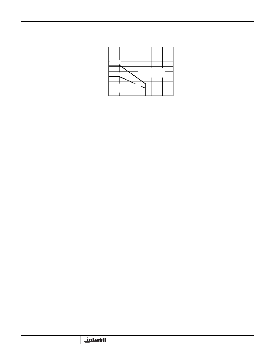
FIGURE 29. PACKAGE POWER DISSIPATION vs AMBIENT TEMPERATURE
Typical Performance Curves (Continued)
1.0
0.9
0.8
0.6
0.4
0.1
0
255075
100
150
AMBIENT TEMPERATURE (°C)
P
O
WER
DIS
S
IP
A
T
ION
(W
)
125
85
JEDEC JESD51-3 LOW EFFECTIVE
THERMAL CONDUCTIVITY TEST BOARD
0.2
0.7
0.3
0.5
625mW
SO8
θ
JA = +160°C/W
SOT23-5/6
θ
JA = +256°C/W
391mW
Gain
BW
×
200MHz
=
(EQ. 1)
EL8102, EL8103
相关PDF资料 |
PDF描述 |
|---|---|
| EL8170FSZ-T7 | IC AMP INSTRU SGL R-R I/O 8-SOIC |
| EL8172FSZ-T7 | IC AMP INSTRU SGL R-R I/O 8-SOIC |
| EL8176FIZ-T7 | IC OP AMP SGL RRIO PREC 6-WLCSP |
| EL8178FWZ-T7 | IC OPAMP SGL R-R I/O SOT23-6 |
| EL8188IW-T7A | IC OPAMP SGL MICROPOWER SOT23-6 |
相关代理商/技术参数 |
参数描述 |
|---|---|
| EL8102IS-T7 | 功能描述:IC OP AMP 500MHZ R-R 8-SOIC RoHS:否 类别:集成电路 (IC) >> Linear - Amplifiers - Instrumentation 系列:- 标准包装:50 系列:- 放大器类型:通用 电路数:2 输出类型:满摆幅 转换速率:1.8 V/µs 增益带宽积:6.5MHz -3db带宽:4.5MHz 电流 - 输入偏压:5nA 电压 - 输入偏移:100µV 电流 - 电源:65µA 电流 - 输出 / 通道:35mA 电压 - 电源,单路/双路(±):1.8 V ~ 5.25 V,±0.9 V ~ 2.625 V 工作温度:-40°C ~ 85°C 安装类型:表面贴装 封装/外壳:10-TFSOP,10-MSOP(0.118",3.00mm 宽) 供应商设备封装:10-MSOP 包装:管件 |
| EL8102ISZ | 功能描述:运算放大器 - 运放 EL8102ISZ 500MHZ R2R AMP RoHS:否 制造商:STMicroelectronics 通道数量:4 共模抑制比(最小值):63 dB 输入补偿电压:1 mV 输入偏流(最大值):10 pA 工作电源电压:2.7 V to 5.5 V 安装风格:SMD/SMT 封装 / 箱体:QFN-16 转换速度:0.89 V/us 关闭:No 输出电流:55 mA 最大工作温度:+ 125 C 封装:Reel |
| EL8102ISZ-T13 | 功能描述:运算放大器 - 运放 EL8102ISZ 500MHZ R2R AMP RoHS:否 制造商:STMicroelectronics 通道数量:4 共模抑制比(最小值):63 dB 输入补偿电压:1 mV 输入偏流(最大值):10 pA 工作电源电压:2.7 V to 5.5 V 安装风格:SMD/SMT 封装 / 箱体:QFN-16 转换速度:0.89 V/us 关闭:No 输出电流:55 mA 最大工作温度:+ 125 C 封装:Reel |
| EL8102ISZ-T7 | 功能描述:运算放大器 - 运放 EL8102ISZ 500MHZ R2R AMP RoHS:否 制造商:STMicroelectronics 通道数量:4 共模抑制比(最小值):63 dB 输入补偿电压:1 mV 输入偏流(最大值):10 pA 工作电源电压:2.7 V to 5.5 V 安装风格:SMD/SMT 封装 / 箱体:QFN-16 转换速度:0.89 V/us 关闭:No 输出电流:55 mA 最大工作温度:+ 125 C 封装:Reel |
| EL8102IW-T7 | 功能描述:IC OP AMP 500MHZ R-R SOT23-6 RoHS:否 类别:集成电路 (IC) >> Linear - Amplifiers - Instrumentation 系列:- 标准包装:1,000 系列:- 放大器类型:电压反馈 电路数:4 输出类型:满摆幅 转换速率:33 V/µs 增益带宽积:20MHz -3db带宽:30MHz 电流 - 输入偏压:2nA 电压 - 输入偏移:3000µV 电流 - 电源:2.5mA 电流 - 输出 / 通道:30mA 电压 - 电源,单路/双路(±):4.5 V ~ 16.5 V,±2.25 V ~ 8.25 V 工作温度:-40°C ~ 85°C 安装类型:表面贴装 封装/外壳:14-SOIC(0.154",3.90mm 宽) 供应商设备封装:14-SOIC 包装:带卷 (TR) |
发布紧急采购,3分钟左右您将得到回复。