参数资料
| 型号: | EL8172FSZ-T7 |
| 厂商: | Intersil |
| 文件页数: | 3/13页 |
| 文件大小: | 0K |
| 描述: | IC AMP INSTRU SGL R-R I/O 8-SOIC |
| 标准包装: | 1,000 |
| 放大器类型: | 仪表 |
| 电路数: | 1 |
| 输出类型: | 满摆幅 |
| 转换速率: | 0.55 V/µs |
| -3db带宽: | 170kHz |
| 电流 - 输入偏压: | 10pA |
| 电压 - 输入偏移: | 70µV |
| 电流 - 电源: | 65µA |
| 电流 - 输出 / 通道: | 32mA |
| 电压 - 电源,单路/双路(±): | 2.4 V ~ 5.5 V |
| 工作温度: | -40°C ~ 125°C |
| 安装类型: | 表面贴装 |
| 封装/外壳: | 8-SOIC(0.154",3.90mm 宽) |
| 供应商设备封装: | 8-SOIC |
| 包装: | 带卷 (TR) |
11
FN6293.5
July 27, 2009
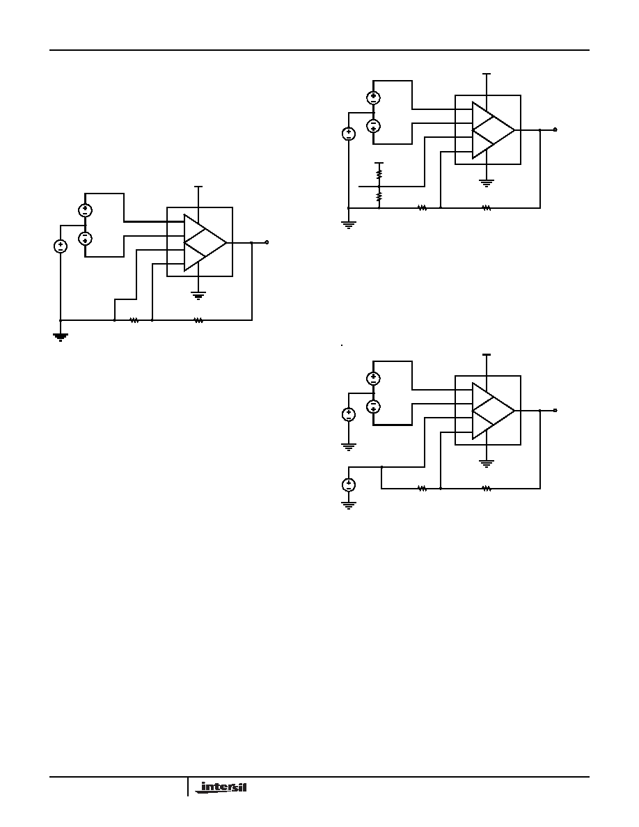
Gain Setting
VIN, the potential difference across IN+ and IN-, is replicated
(less the input offset voltage) across FB+ and FB-. The
obsession of the EL8171 and EL8172 in-amp is to maintain
the differential voltage across FB+ and FB- equal to IN+ and
IN-; (FB+ - FB-) = (IN+ - IN-). Consequently, the transfer
function can be derived. The gain of the EL8171 and EL8172
is set by two external resistors, the feedback resistor RF, and
the gain resistor RG.
In Figure 37, the FB+ pin and one end of resistor RG are
connected to GND. With this configuration, Equation 1 is
only true for a positive swing in VIN; negative input swings
will be ignored and the output will be at ground.
Reference Connection
Unlike a three-op amp instrumentation amplifier, a finite
series resistance seen at the REF terminal does not degrade
the EL8171 and EL8172's high CMRR performance,
eliminating the need for an additional external buffer
amplifier. Circuit 2 (Figure 38) uses the FB+ pin to provide a
high impedance REF terminal.
The FB+ pin is used as a REF terminal to center or to adjust
the output. Because the FB+ pin is a high impedance input,
an economical resistor divider can be used to set the voltage
at the REF terminal without degrading or affecting the CMRR
performance. Any voltage applied to the REF terminal will
shift VOUT by VREF times the closed loop gain, which is set
by resistors RF and RG. See Circuit 2 (Figure 38). Note that
any noise or unwanted signals on the reference supply will
be amplified at the output according to Equation 2.
The FB+ pin can also be connected to the other end of resistor,
RG. See Circuit 3 (Figure 39). Keeping the basic concept that
the EL8171 and EL8172 in-amps maintain constant differential
voltage across the input terminals and feedback terminals (IN+
- IN- = FB+ - FB-), the transfer function of Circuit 3 can be
derived. Note that the VREF gain term is eliminated and
susceptibility to external noise is reduced, however the VREF
source must be capable of sourcing or sinking the feedback
current from VOUT through RF and RG.
External Resistor Mismatches
Because of the independent pair of feedback terminals
provided by the EL8171 and EL8172, the CMRR is not
degraded by any resistor mismatches. Hence, unlike a three op
amp and especially a two op amp in-amp, the EL8171 and
EL8172 reduce the cost of external components by allowing the
use of 1% or more tolerance resistors without sacrificing CMRR
performance. The EL8171 and EL8172 CMRR will be
maintained regardless of the tolerance of the resistors used.
Gain Error and Accuracy
The EL8172 has a Gain Error (EG) of 0.2% typical. The
EL8171 has an EG of 0.15% typical. The gain error indicated
in the “Electrical Specifications” table on page 2 is the inherent
gain error of the EL8171 and EL8172 and does not include
1
3
2
8
5
4
7
6
+
-
+
-
IN+
IN-
FB+
FB-
V+
V-
2.4V TO 5.5V
RF
RG
VOUT
EL8171/2
VCM
VIN/2
FIGURE 37. CIRCUIT 1 - GAIN IS BY EXTERNAL RESISTORS
RF AND RG
V
OUT
1
R
F
R
G
--------
+
V
IN
=
(EQ. 1)
FIGURE 38. CIRCUIT 2 - GAIN SETTING AND REFERENCE
CONNECTION
1
3
2
8
5
4
7
6
+
-
+
-
IN+
IN-
FB+
FB-
V+
V-
2.4V TO 5.5V
RF
RG
VOUT
EL8171/2
VCM
VIN/2
R1
R2
REF
2.4V TO 5.5V
V
OUT
1
R
F
R
G
--------
+
V
IN
()
1
R
F
R
G
--------
+
V
REF
()
+
=
(EQ. 2)
1
3
2
8
5
4
7
6
+
-
+
-
IN+
IN-
FB+
FB-
V+
V-
2.4V TO 5.5V
RF
RG
VOUT
EL8171/2
VCM
VIN/2
VREF
FIGURE 39. CIRCUIT 3 - REFERENCE CONNECTION WITH AN
AVAILABLE VREF
V
OUT
1
R
F
R
G
--------
+
V
IN
()
V
REF
()
+
=
(EQ. 3)
EL8171, EL8172
相关PDF资料 |
PDF描述 |
|---|---|
| EL8176FIZ-T7 | IC OP AMP SGL RRIO PREC 6-WLCSP |
| EL8178FWZ-T7 | IC OPAMP SGL R-R I/O SOT23-6 |
| EL8188IW-T7A | IC OPAMP SGL MICROPOWER SOT23-6 |
| EL8300IUZ-T13 | IC AMP TRIPLE R-R 200MHZ 16-QSOP |
| EL8302IU-T13 | IC AMP TRIPLE R-R 500MHZ 16-QSOP |
相关代理商/技术参数 |
参数描述 |
|---|---|
| EL8172FSZ-T7A | 功能描述:仪表放大器 EL8172FSZ MICROPWR SINGL SUPY R2R I/O RoHS:否 制造商:Texas Instruments 通道数量: 输入补偿电压:150 V 可用增益调整: 最大输入电阻:10 kOhms 共模抑制比(最小值):88 dB 工作电源电压:2.7 V to 36 V 电源电流:200 uA 最大工作温度:+ 125 C 最小工作温度:- 40 C 封装 / 箱体:MSOP-8 封装:Bulk |
| EL8172IS | 功能描述:IC AMP INSTR SGL R-R I/O 8-SOIC RoHS:否 类别:集成电路 (IC) >> Linear - Amplifiers - Instrumentation 系列:- 标准包装:50 系列:LinCMOS™ 放大器类型:通用 电路数:4 输出类型:- 转换速率:0.05 V/µs 增益带宽积:110kHz -3db带宽:- 电流 - 输入偏压:0.7pA 电压 - 输入偏移:210µV 电流 - 电源:57µA 电流 - 输出 / 通道:30mA 电压 - 电源,单路/双路(±):3 V ~ 16 V,±1.5 V ~ 8 V 工作温度:-40°C ~ 85°C 安装类型:表面贴装 封装/外壳:14-SOIC(0.154",3.90mm 宽) 供应商设备封装:14-SOIC 包装:管件 产品目录页面:865 (CN2011-ZH PDF) 其它名称:296-1834296-1834-5 |
| EL8172IS-T13 | 功能描述:IC AMP INSTR SGL R-R I/O 8-SOIC RoHS:否 类别:集成电路 (IC) >> Linear - Amplifiers - Instrumentation 系列:- 标准包装:50 系列:LinCMOS™ 放大器类型:通用 电路数:4 输出类型:- 转换速率:0.05 V/µs 增益带宽积:110kHz -3db带宽:- 电流 - 输入偏压:0.7pA 电压 - 输入偏移:210µV 电流 - 电源:57µA 电流 - 输出 / 通道:30mA 电压 - 电源,单路/双路(±):3 V ~ 16 V,±1.5 V ~ 8 V 工作温度:-40°C ~ 85°C 安装类型:表面贴装 封装/外壳:14-SOIC(0.154",3.90mm 宽) 供应商设备封装:14-SOIC 包装:管件 产品目录页面:865 (CN2011-ZH PDF) 其它名称:296-1834296-1834-5 |
| EL8172IS-T7 | 功能描述:IC AMP INSTR SGL R-R I/O 8-SOIC RoHS:否 类别:集成电路 (IC) >> Linear - Amplifiers - Instrumentation 系列:- 标准包装:50 系列:LinCMOS™ 放大器类型:通用 电路数:4 输出类型:- 转换速率:0.05 V/µs 增益带宽积:110kHz -3db带宽:- 电流 - 输入偏压:0.7pA 电压 - 输入偏移:210µV 电流 - 电源:57µA 电流 - 输出 / 通道:30mA 电压 - 电源,单路/双路(±):3 V ~ 16 V,±1.5 V ~ 8 V 工作温度:-40°C ~ 85°C 安装类型:表面贴装 封装/外壳:14-SOIC(0.154",3.90mm 宽) 供应商设备封装:14-SOIC 包装:管件 产品目录页面:865 (CN2011-ZH PDF) 其它名称:296-1834296-1834-5 |
| EL8172ISZ | 功能描述:IC AMP INSTR SGL R-R I/O 8-SOIC RoHS:是 类别:集成电路 (IC) >> Linear - Amplifiers - Instrumentation 系列:- 标准包装:50 系列:LinCMOS™ 放大器类型:通用 电路数:4 输出类型:- 转换速率:0.05 V/µs 增益带宽积:110kHz -3db带宽:- 电流 - 输入偏压:0.7pA 电压 - 输入偏移:210µV 电流 - 电源:57µA 电流 - 输出 / 通道:30mA 电压 - 电源,单路/双路(±):3 V ~ 16 V,±1.5 V ~ 8 V 工作温度:-40°C ~ 85°C 安装类型:表面贴装 封装/外壳:14-SOIC(0.154",3.90mm 宽) 供应商设备封装:14-SOIC 包装:管件 产品目录页面:865 (CN2011-ZH PDF) 其它名称:296-1834296-1834-5 |
发布紧急采购,3分钟左右您将得到回复。