参数资料
| 型号: | EL9112ILZ-T13 |
| 厂商: | Intersil |
| 文件页数: | 2/13页 |
| 文件大小: | 0K |
| 描述: | IC DIFF RCVR/EQUALZR TRPL 28-QFN |
| 标准包装: | 2,500 |
| 类型: | 接收器 |
| 驱动器/接收器数: | 0/3 |
| 规程: | 双绞线 |
| 电源电压: | 5V |
| 安装类型: | 表面贴装 |
| 封装/外壳: | 28-VFQFN 裸露焊盘 |
| 供应商设备封装: | * |
| 包装: | 带卷 (TR) |
10
FN7450.4
May 9, 2007
Applications Information
Logic Control
The EL9112 has two logical input pins, Chip Enable
(ENABLE) and Switch Gain (X2). The logic circuits all have a
nominal threshold of 1.1V above the potential of the logic
reference pin (VREF). In most applications it is expected that
this chip will run from a +5V, 0V, -5V supply system with logic
being run between 0V and +5V. In this case the logic
reference voltage should be tied to the 0V supply. If the logic
is referenced to the -5V rail, then the logic reference should
be connected to -5V. The logic reference pin sources about
60A and this will rise to about 200A if all inputs are true
(positive).
The logic inputs all source up to 10A when they are held at
the logic reference level. When taken positive, the inputs
sink a current dependent on the high level, up to 50A for a
high level 5V above the reference level.
The logic inputs, if not used, should be tied to the
appropriate voltage in order to define their state.
Control Reference and Signal Reference
Analog control voltages are required to set the equalizer and
contrast levels. These signals are voltages in the range 0V -
1V, which are referenced to the control reference pin. It is
expected that the control reference pin will be tied to 0V and
the control voltage will vary from 0V to 1V. It is; however,
acceptable to connect the control reference to any potential
between -5V and 0V to which the control voltages are
referenced.
The control voltage pins themselves are high impedance.
The control reference pin will source between 0A and
200A depending on the control voltages being applied.
The control reference and logic reference effectively remove
the need for the 0V rail and operation from ±5V (or 0V and
10V) only is possible. However we still need a further
reference to define the 0V level of the single ended output
signal. The reference for the output signal is provided by the
0V pin. The output stage cannot pull fully up or down to
either supply so it is important that the reference is
positioned to allow full output swing. The 0V reference
should be tied to a 'quiet ground' as any noise on this pin is
transferred directly to the output. The 0V pin is a high
impedance pin and draws DC bias currents of a few A and
similar levels of AC current.
Equalizing
When transmitting a signal across a twisted pair cable, the
high frequency (above 1MHz) information is attenuated
more significantly than the information at low frequencies.
The attenuation is predominantly due to resistive skin effect
losses and has a loss curve which depends on the resistivity
of the conductor, surface condition of the wire and the wire
diameter. For the range of high performance twisted pair
cables based on 24awg copper wire (CAT-5 etc.) these
parameters vary only a little between cable types, and in
general cables exhibit the same frequency dependence of
loss. (The lower loss cables can be compared with
somewhat longer lengths of their more lossy brothers.) This
enables a single equalizing law equation to be built into the
EL9112.
With a control voltage applied between pins VCTRL and
VREF, the frequency dependence of the equalization is
shown in Figure 8. The equalization matches the cable loss
up to about 100MHz. Above this, system gain is rolled off
rapidly to reduce noise bandwidth. The roll-off occurs more
rapidly for higher control voltages, thus the system (cable +
equalizer) bandwidth reduces as the cable length increases.
This is desirable, as noise becomes an increasing issue as
the equalization increases.
Contrast
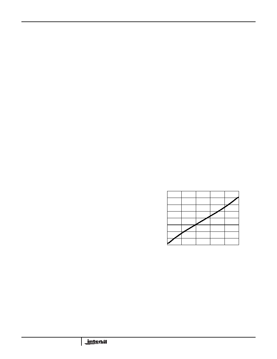
By varying the voltage between pins VGAIN and VREF, the
gain of the signal path can be changed in the ratio 4:1. The
gain change varies almost linearly with control voltage. For
normal operation it is anticipated the X2 mode will be
selected and the output load will be back matched. A unity
gain to the output load will then be achieved with a gain
control voltage of about 0.35V. This allows the gain to be
trimmed up or down by 6dB to compensate for any gain/loss
errors that affect the contrast of the video signal. Figure 26
shows an example plot of the gain to the load with gain
control voltage.
FIGURE 26. VARIATION OF GAIN WITH GAIN CONTROL
VOLTAGE
Common Mode Sync Decoding
The EL9111 features common mode decoding to allow
horizontal and vertical synchronization information, which
has been encoded on the three differential inputs by the
EL4543, to be decoded. The entire RGB video signal can
therefore be transmitted, along with the associated
synchronization information, by using just three twisted
pairs.
00.8
VGAIN
0.4
1
2.0
1.8
1.4
1.0
0.6
0.4
GAI
N
(
V
)
0.6
0.2
1.6
1.2
0.8
EL9111, EL9112
相关PDF资料 |
PDF描述 |
|---|---|
| VE-B72-MW-F1 | CONVERTER MOD DC/DC 15V 100W |
| MAX170DCWE+T | IC ADC 12BIT SERIAL 16-SOIC |
| EL9111ILZ-T7 | IC DIFF RCVR/EQUALZR TRPL 28-QFN |
| VE-B71-MW-F4 | CONVERTER MOD DC/DC 12V 100W |
| MS27508E14A15SA | CONN RCPT 15POS BOX MNT W/SCKT |
相关代理商/技术参数 |
参数描述 |
|---|---|
| EL9112ILZ-T7 | 功能描述:总线接收器 EL9112ILZ TRPL DIFFR NTLCVR/EQUALIZER RoHS:否 制造商:Texas Instruments 接收机数量:4 接收机信号类型:Differential 接口类型:EIA/TIA-422-B, V.11 工作电源电压:3.3 V 最大工作温度:+ 85 C 最小工作温度:- 40 C 封装 / 箱体:TSSOP-16 封装:Reel |
| EL9115 | 制造商:INTERSIL 制造商全称:Intersil Corporation 功能描述:Triple Analog Video Delay Line |
| EL9115_06 | 制造商:INTERSIL 制造商全称:Intersil Corporation 功能描述:Triple Analog Video Delay Line |
| EL9115_08 | 制造商:INTERSIL 制造商全称:Intersil Corporation 功能描述:Triple Analog Video Delay Line |
| EL9115_09 | 制造商:INTERSIL 制造商全称:Intersil Corporation 功能描述:Triple Analog Video Delay Line |
发布紧急采购,3分钟左右您将得到回复。