- 您现在的位置:买卖IC网 > PDF目录93403 > EM4100A6CB2RC Single 12V Input Supply Dual Regulator - Synchronous Rectified Buck PWM and Linear Power Controller; Temperature Range: -40°C to 85°C; Package: 16-QFN PDF资料下载
参数资料
| 型号: | EM4100A6CB2RC |
| 元件分类: | 线性稳压 |
| 英文描述: | Single 12V Input Supply Dual Regulator - Synchronous Rectified Buck PWM and Linear Power Controller; Temperature Range: -40°C to 85°C; Package: 16-QFN |
| 中文描述: | 模拟杂项 |
| 文件页数: | 5/9页 |
| 文件大小: | 78K |
| 代理商: | EM4100A6CB2RC |

EM4100
Copyright
2002, EM Microelectronic-Marin SA
5
www.emmicroelectronic.com
Memory Array for Manchester & Bi-Phase encoding ICs
The EM4100 contains 64 bits divided in five groups of
information. 9 bits are used for the header, 10 row parity
bits (P0-P9), 4 column parity bits (PC0-PC3), 40 data bits
(D00-D93), and 1 stop bit set to logic 0.
111111
111
9 header bits
8 version bits or
D00
D01 D02 D03
P0
customer ID
D10
D11 D12 D13
P1
D20
D21 D22 D23
P2
32 data bits
D30
D31 D32 D33
P3
D40
D41 D42 D43
P4
D50
D51 D52 D53
P5
D60
D61 D62 D63
P6
D70
D71 D72 D73
P7
D80
D81 D82 D83
P8
D90
D91 D92 D93
P9
10 line parity
PC0
PC1 PC2 PC3 S0
bits
4 column parity bits
The header is composed of the 9 first bits which are all
mask programmed to "1".
Due to the data and parity
organisation, this sequence cannot be reproduced in the
data string. The header is followed by 10 groups of 4 data
bits allowing 100 billion combinations and 1 even row
parity bit. Then, the last group consists of 4 event column
parity bits without row parity bit. S0 is a stop bit which is
written to "0"
Bits D00 to D03 and bits D10 to D13 are customer specific
identification.
These 64 bits are outputted serially in order to control the
modulator. When the 64 bits data string is outputted, the
output sequence is repeated continuously until power goes
off.
Memory Array for PSK encoding ICs
The PSK coded IC's are programmed with odd parity for
P0 and P1 and always with a logic zero.
The parity bits from P2 to P9 are even.
The column parity PC0 to PC3 are calculated including the
version bits and are even parity bits.
Code Description
Manchester
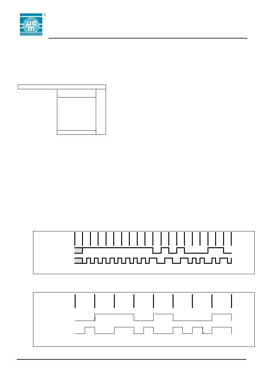
There is always a transition from ON to OFF or from OFF
to ON in the middle of bit period. At the transition from
logic bit “1” to logic bit “0” or logic bit “0” to logic bit “1” the
phase change. Value high of data stream presented below
modulator
switch
OFF,
low
represents
switch
ON
(see Fig. 6).
Biphase Code
At the beginning of each bit, a transition will occur. A logic
bit “1” will keep its state for the whole bit duration and a
logic bit “0” will show a transition in the middle of the bit
duration (see Fig. 7).
PSK Code
Modulation switch goes ON and OFF alternately every
period of carrier frequency. When a phase shift occurs, a
logical "0" is read from the memory. If no shift phase
occurs after a data rate cycle, a logical "1" is read
(see Fig. 8).
Manchester Code
X
1
0
1
0
1
0
1
0
Modulation control "low" means high current
Binary data
Memory output
Modulator control
Fig. 6
Biphase Code
0
1101
00
1
Binary data
Memory output
Modulator control
Modulation control "low" means high current
Fig. 7
相关PDF资料 |
PDF描述 |
|---|---|
| EM4100A6CI2LB | ZVS Full Bridge PWM Controller; Temperature Range: -25°C to 85°C; Package: 28-SOIC |
| EM4100A6CI2LC | Analog Miscellaneous |
| EM4100A6CX | ZVS Full Bridge PWM Controller; Temperature Range: -25°C to 85°C; Package: 28-QFN T&R |
| EM4100A6CY | ZVS Full Bridge PWM Controller; Temperature Range: -40°C to 85°C; Package: 28-SOIC |
| EM4100C4CI2LC | Optimized Multiphase PWM Controller with 6-Bit DAC for VR10.X Application; Temperature Range: 0°C to 70°C; Package: 28-SOIC |
相关代理商/技术参数 |
参数描述 |
|---|---|
| EM4100A6CI2LB | 制造商:未知厂家 制造商全称:未知厂家 功能描述:Analog Miscellaneous |
| EM4100A6CI2LC | 制造商:未知厂家 制造商全称:未知厂家 功能描述:Analog Miscellaneous |
| EM4100A6CX | 制造商:未知厂家 制造商全称:未知厂家 功能描述:Analog Miscellaneous |
| EM4100A6CY | 制造商:未知厂家 制造商全称:未知厂家 功能描述:Analog Miscellaneous |
| EM4100A6WP11 | 制造商:EMMICRO 制造商全称:EM Microelectronic - MARIN SA 功能描述:Read Only Contactless Identification Device |
发布紧急采购,3分钟左右您将得到回复。